TCL script Vivado Project Tutorial

Vivado is the Hardware Development suite used to implement a design in Xilinx FPGA. In this post, is reported how to create a Vivado project using the Graphical User Interface (GUI). This is the fastest and common approach to creating a project in Vivado.

Vivado GUI performs the complete design flow for a Xilinx FPGA:

  • Simulate
  • Synthesize
  • Map
  • Route
  • Analyze Timing
  • Create a bit-stream FPGA configuration File
  • Configure FPGA
  • Debug the FPGA using ILA (Integrated Logic Analyzer)

Vivado also allows the user to perform the design flow using TCL language.

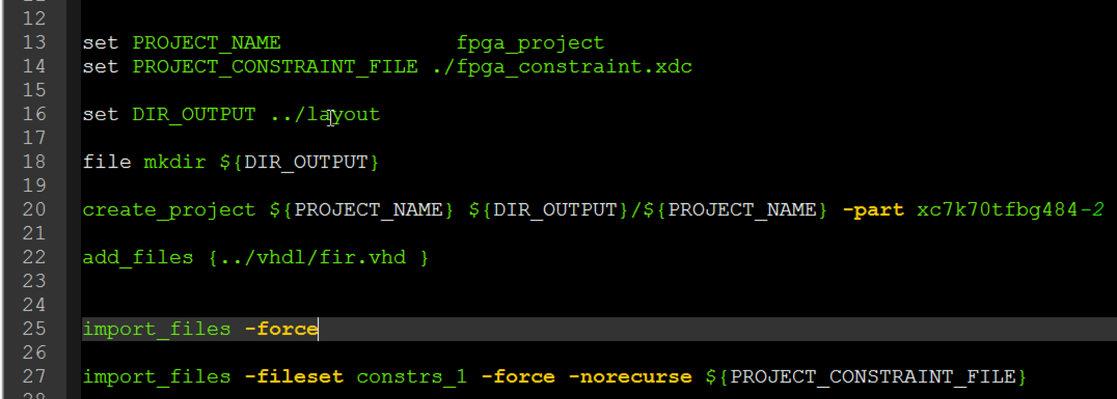
The TCL scripting is very useful to create a compact and deterministic way to realize a layout flow in FPGA. This approach is adopted by expert users. You should take it into consideration even if you are not an expert. In this post, we are going to see a simple example that can be used as a template for the Vivado TCL project script. The project created using the TCL script can be also opened and edited using the Vivado GUI. All the analysis as timing, area, etc can be performed using GUI after design flow completion.

Read More

Vivado Project Tutorial

Vivado is the Hardware Development suite used to create a VHDL, Verilog, or any other HDL design on the latest Xilinx FPGA. In other words, when you need to translate your VHDL design into a configuration file to be downloaded into a Xilinx FPGA, you need Vivado framework.

Vivado is an integrated tool that allows you to perform the complete design flow for a Xilinx FPGA:

  • Simulate
  • Synthesize
  • Map
  • Route
  • Analyze Timing
  • Create a bit-stream FPGA configuration File
  • Configure FPGA
  • Debug the FPGA using ILA (Integrated Logic Analyzer)

In this post, we are going to see how to initialize Vivado tool to be ready to create an FPGA bit-stream programming file, starting from a simple VHDL code.

Read More

SPI Slave VHDL design

In this post, we are going to design the VHDL code for the SPI slave module that can be connected to an SPI master.

You will see:

  • SPI slave typical protocol
  • SPI slave four wire hardware design
  • VHDL implementation of a 4-wire SPI slave
  • VHDL simulation of SPI Master-slave communication
  • Layout consideration for SPI slave implementation

Serial Peripheral Interface Introduction – SPI Master / Slave

In a previous post, we introduced the SPI master controller module. The SPI master originates the frame for reading and writing multiple SPI slave devices using individual slave select (SS) lines.

The SPI is a three or four-wire serial bus as you can see in Figure 1

Figure 1 – SPI Master-Slave 4-wire connection example (image Wikipedia)
Read More

How to Declare a Procedure in VHDL

VHDL can implement procedures. Even if the VHDL is a hardware description language, it can define procedures like a common programming language.

When we use a procedure, we always need to take in mind how the procedure code is translated in hardware implementation.

In this post, we will address the classical use of a procedure. It is a software approach, not a hardware approach.

First of all, as a golden rule, we need to take in mind what my professor of computer science used to repeat to me during the lessons at university:

When you need to write twice a piece of code, write a procedure or function.

Read More

18th Annual Embedded Systems Workshop

IEEE Computer Society in collaboration with the IEEE Education Society (South East Michigan Chapters) is offering TWO half-day workshops on Embedded Systems on Saturday, October 17th & 24th, 2020.

This workshop is open to all industry professionals, both experienced and newly minted engineers, as well as students. This is the 18th year that the event is being held.

The aim is to disseminate knowledge, directly benefitting the IEEE members, at the same time improve the technology skills pool, indirectly boosting the Michigan economy.

Speakers and experts from the embedded systems industry will be making presentations, and will also be available for discussions and networking throughout the day. In addition to the technical presentations, there will be industry information display and professional recruitment sessions. Use this opportunity for virtual networking with other engineers, industry experts, and embedded enthusiasts.

I’ll partecipate on October 24th talking about:

The role of VHDL in embedded systems the advantages of a Hardware Description Language

here the link to the conference: https://bit.ly/embed2020

Multiplier optimization in VHDL

When FPGAs do not implement a multiplier HW macro

The modern FPGAs implement multiplication using a dedicated hardware resource. Such dedicated hardware resource generally implements 18×18 multiply and accumulate function. Many FPGAs use two 9×9 multiplier IP to implement a single 18×18 multiplier macro. It depends on the technology you are using.

Depending on the technology and FPGA you are using it is also possible to have no multiplier at all as dedicated IP. In this case, if you need to perform a multiplication it could be a problem. Multiplication is a very demanding operator in term of area and timing resources, so you need to pay attention to the operand number of bits in order to minimize the area and timing impact on your FPGA.

Read More

How to implement a Serial to Parallel converter

Parallelize after serializing

In this post, we analyzed the VHDL code for a parallel to serial converter. This approach is very useful in interfacing different devices. Many FPGA vendors like Xilinx, Intel/Altera give us the possibility to use internal serializer-deserializer such as a serial transceiver. In this post, we want to implement the complementary interface of the parallel to serial interface. We will see how to implement the VHDL code for a serial to parallel interface in order to get back the parallel data bus we sent in the transmitter device. In other words, we will implement the VHDL block in the of the bottom right of Figure1

Figure 1 FPGA connection Parallel vs Serial

Read More

How to implement a Parallel to Serial converter

Connecting two devices

When we need to transfer data from two different devices, the simple way is to use the minimum numbers of wires. For instance, if we need to transfer a data bus of 16 bits between two different FPGA at a rate of 1 MHz, we need to connect at least

16-bit data + 1 bit enable + 1 bit clock = 18 wires running @ 1 MHz. As you can see, these are a lot of wires! Moreover, a skew between the bits in the parallel data bus can affect the connection integrity.

Figure 1 FPGA connection Parallel vs Serial

Another method for data transfer, could be to serialize the parallel data using less connection.

Read More

How to compensate amplitude and phase imbalance in VHDL

The real mixing refers to the translation of a signal in frequency by multiplying it with a single oscillator signal as in figure below

Figure 1 – Typical I/Q modulator-demodulator architecture

This approach is performed using the I/Q modulator technique. The I/Q modulator is a critical component in the signal chain for modern digital transmitters. An I/Q modulators perform the frequency translation that mixes the baseband signal to the desired location in the RF spectrum. An I/Q modulator consists of a local oscillator (LO) input that is split into in-phase (I) and quadrature (Q) components that are separated by 90°. An example of I/Q modulator is given in [3] These two signals drive separate mixers that are also driven by I and Q baseband signals processor.

Read More