In this post, we are going to design the VHDL code for the SPI slave module that can be connected to an SPI master.
You will see:
- SPI slave typical protocol
- SPI slave four wire hardware design
- VHDL implementation of a 4-wire SPI slave
- VHDL simulation of SPI Master-slave communication
- Layout consideration for SPI slave implementation
Serial Peripheral Interface Introduction – SPI Master / Slave
In a previous post, we introduced the SPI master controller module. The SPI master originates the frame for reading and writing multiple SPI slave devices using individual slave select (SS) lines.
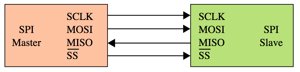
The SPI is a three or four-wire serial bus as you can see in Figure 1
For further information see https://en.wikipedia.org/wiki/Serial_Peripheral_Interface_Bus
The SPI is, basically, a serial to parallel converter controlled by the SS signal. Input data MOSI (Master Out Serial In) go through an input shift register when the SS control signal is low. When the SS goes from low to high data in the input shift register is ready to be read.
The same approach is related to the MISO (Master In Serial Output) output signal from the slave. In this case, the data in the output shift register is serialized at each clock cycle by shifting the parallel data.
Figure 2 reports the input-output shift register example for input MOSI and output MISO SPI slave signal.

SPI slave design overview
The SPI bus specifies four logic signals:
SCLK : Serial Clock (output from master).
MOSI : Master Output, Slave Input (output from master).
MISO : Master Input, Slave Output (output from slave).
SS : Slave Select (active low, output from master).
You can find alternate naming, but the functionalities are the same.

SPI timing example is shown in Figure 3. The input MOSI can be clocked either on the rising or falling edge of SCKL depending on the polarity CPOL selected. If MOSI is strobed on the rising edge of SCLK, MISO will be clocked on the falling and vice versa.
From Figure 3, when CPOL=1, the SPI slave data input/output change on the falling edge of SCLK. The serial data is shifted on the input shift register on the rising edge of the clock (blue vertical dotted lines) and the output data is serialized shifting the output shift register on the falling edge of the clock (red vertical dotted line).
In the case of CPOL=0, the behavior is similar, taking into account the opposite clock edges.
SPI slave VHDL code implementation
Before going into the SPI slave VHDL code, let’s review the SPI slave architecture of Figure 2 with timing reported in Figure 3
o_busy             : serial data received/transmitted
o_data_parallel    : received parallelized data
i_data_parallel    : parallel data to sent
i_sclk             : serial clock output
i_ss               : slave select
i_mosi             : Master Ouput Serial In (input serial data)
o_miso             : Master In Serial out (output serial data)
the SPI slave VHDL code implements the input and output shift register. The SPI Slave module works with the SCLK input clock and SS input select signal.
When you interface this SPI slave VHDL module with your design components, you must take care of clock domain crossing (CDC) between the SCLK input serial clock of the SPI slave module and the internal clock of your VHDL design.
The signal that shall be used to resynchronize the two clock domains, is the o_busy output signal.
The internal clock that we are going to use in the VHDL design instantiating the SPI slave module, should run faster than the SPI slave clock. Moreover, the SPI slave clock is not a continuous clock.
You can detect the falling edge of the o_busy SPI slave select signal to strobe the parallel data received by the SPI slave module.
You must pay attention to the parallel data to be sent. In this case, the output parallel shift register is loaded on the first SPI clock edge when the SS signal is low. The clock edge depends on the CPOL configuration. In this case, you must guarantee that the parallel data to be shifted is stable before the SS signal goes low.
A possible VHDL implementation of SPI slave is available below
Here below, the VHDL code for the SPI slave module. In the SPI slave module, the i_mosi input serial data is clocked using the i_sclk SPI serial clock.
library ieee;
use ieee.std_logic_1164.all;
use ieee.numeric_std.all;

entity spi_slave is
generic(
	N                     : integer := 2;      -- number of bit to serialize
	CPOL                  : std_logic := '0' );  -- clock polarity
 port (
	o_busy                      : out std_logic;  -- receiving data if '1'
	i_data_parallel             : in  std_logic_vector(N-1 downto 0);  -- data to sent
	o_data_parallel             : out std_logic_vector(N-1 downto 0);  -- received data
	i_sclk                      : in  std_logic;
	i_ss                        : in  std_logic;
	i_mosi                      : in  std_logic;
	o_miso                      : out std_logic);
end spi_slave;

architecture rtl of spi_slave is

signal r_shift_ena                           : std_logic;
signal r_tx_data                             : std_logic_vector(N-2 downto 0);  -- data to sent
signal r_rx_data                             : std_logic_vector(N-1 downto 0);  -- received data

begin
o_data_parallel  <= r_rx_data;
o_busy           <= r_shift_ena;

p_spi_slave_input : process(i_sclk)
begin
	if(i_sclk'event and i_sclk=CPOL) then -- CPOL='0' => falling edge; CPOL='1' => risinge edge
		if(i_ss='0') then
			r_rx_data              <= r_rx_data(N-2 downto 0)&i_mosi;
		end if;
	end if;
end process p_spi_slave_input;

p_spi_slave_output : process(i_sclk,i_ss)
begin
	if(i_ss='1') then
		r_shift_ena            <= '0';
	elsif(i_sclk'event and i_sclk= not CPOL) then -- CPOL='0' => falling edge; CPOL='1' => risinge edge
		r_shift_ena            <= '1';
		if(r_shift_ena='0') then
			o_miso                 <= i_data_parallel(N-1);
			r_tx_data              <= i_data_parallel(N-2 downto 0);
		else
			o_miso                 <= r_tx_data(N-2);
			r_tx_data              <= r_tx_data(N-3 downto 0)&'0';
		end if;
	end if;
end process p_spi_slave_output;

end rtl;
The module connected to the SPI slave can use the port signal o_busy to detect when the input frame has been received. It can be easily done just by detecting the falling edge of the signal. To detect the falling edge of busy you can refer to this post where you can find how to implement a good edge detector
SPI slave simulation results

Figure 4 reports a simulation of the SPI slave module. As you can see the output port “o_data_parallel” contains the parallel value of the received serial data. The simulation “o_data_parallel” reports the MOSI serial data parallelized in the output register. Data is valid on the falling edge of the “o_busy” signal.
The bit numbering is the first bit is the MSB (most significant bit).
The input port “i_data_parallel” can be used to send back to the SPI master data from the internal design. In the simulation, the test-bench parallelize the MISO serial data into the “r_miso_parallel” test register to verify the correct behavior of the SPI-slave module.
You can easily customize the VHDL of the SPI slave to match your requirement. For instance, you can connect the SPI slave to an internal control logic that interprets the “o_data_parallel” value and performs read/write operation to an internal control register.
As you can understand, if you need to read out a value, you can decode a read command from the input data stream and, on the next command, you can send back the read value on the MISO serial line. In other words, the read value has one command delay latency. This is a common behavior in the SPI link.
SPI slave layout results
This section reports a layout of the SPI slave VHDL using Intel/Altera Quartus II on Terasic DE0 FPGA. The layout is implemented using N=4.

In this example, the value of 4 is used only to better analyze the output design diagram in Figure 5.
The SPI protocol is driven by the serial clock “i_sclk”. Even if the serial SPI I/O stream is synchronous with respect to the serial clock, when the signals i_sclk , i_ss, i_mosi input in the FPGA, the internal logic must be considered asynchronous.
The o_miso signal is synchronous with respect to the i_sclk.
In this case, you must pay attention to the constraints related to such signals.
From the SPI slave VHDL code and from the figure reporting the related layout, is clear that “i_ss” is used as asynchronous reset for the control signal that is used to enable the input and output shift register.
It is also used to drive the o_busy signal used to detect the completion of the SPI slave serial data burst. So, after the layout, mostly if your device is congested in terms of FPGA area resources, you must control if the skew between the input signal is acceptable considering the serial clock constraint.
This can be done using input constraint on the SPI slave input pin to specify the maximum delay from the FPGA pad to SPI internal registers. Another possible solution is to fix the SPI slave register location close to the FPGA pads to minimize the routing connection of this section.
Conclusion
In this post, we designed a 4-wire SPI slave VHDL module. A Modelsim simulation has been reported to verify SPI slave correct behavior.
The last section is described an example of implementation on FPGA that pointed out the typical layout consideration to be taken into account when the SPI slave is implemented on an FPGA
References
[1] https://en.wikipedia.org/wiki/Serial_Peripheral_Interface_Bus
[2] Download Intel® Quartus® Prime Software
[3] Altera DE0 Board
It’s very good article, but I think, that comment in line number 42 is incorrect. In’s need to be “CPOL=’0′ => rising edge; CPOL=’1′ => falling edge”
thank you for your feedback.
This setting has half clock period as setup time