Vivado is the Hardware Development suite used to create a VHDL, Verilog, or any other HDL design on the latest Xilinx FPGA. In other words, when you need to translate your VHDL design into a configuration file to be downloaded into a Xilinx FPGA, you need Vivado framework.
Vivado is an integrated tool that allows you to perform the complete design flow for a Xilinx FPGA:
- Simulate
- Synthesize
- Map
- Route
- Analyze Timing
- Create a bit-stream FPGA configuration File
- Configure FPGA
- Debug the FPGA using ILA (Integrated Logic Analyzer)
In this post, we are going to see how to initialize Vivado tool to be ready to create an FPGA bit-stream programming file, starting from a simple VHDL code.
Using Vivado you can create and manage the soft and hard IP provided for the FPGA. In the next section, we are going to see only how to set up a simple project starting from VHDL source code.
Vivado also allows the user to perform the design flow using the shell and TCL language.
The TCL scripting is very useful to create a compact and deterministic way to realize a layout flow in FPGA. This approach is used by expert users, by the way, you should take it into consideration even if you are not an expert.
Starting a new Vivado project
Every FPGA hardware development tool needs to create a project. A project contains all the information the different development FPGA software need to realize a design in FPGA. This concept is valid for all FPGA development tools, i.e. Intel Quartus, Lattice ICE Cube, Microsemi Libero SoC, not only for Xilinx Vivado.
When you run Vivado, the starting window is reported in Figure 1.
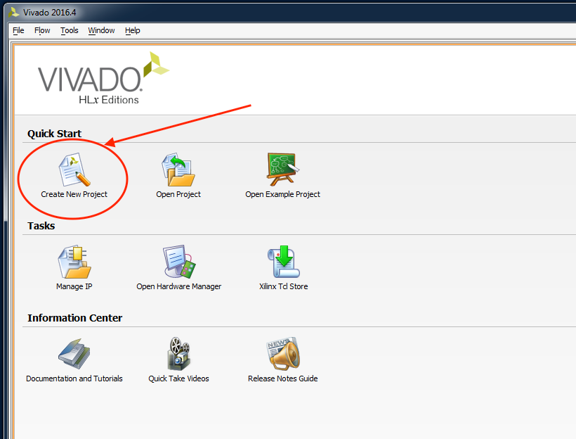
Figure 1 Vivado Starting window Create New Project
We need to “Create New Project” as in Figure 1 by clicking on the relative icon.
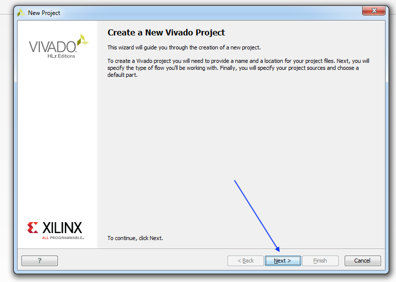
Figure 2 Create a New Vivado Project window
Create New Project
Clicking on the “Create New Project” activate the “New Vivado Project” Wizard, so click next on the opened window.
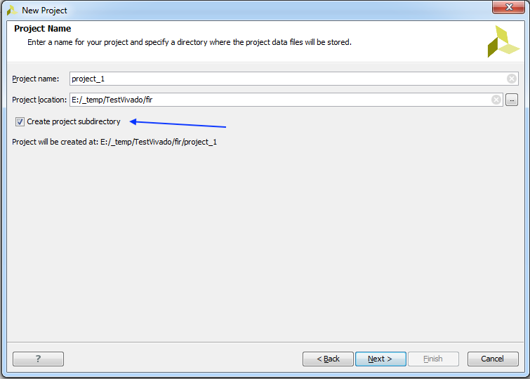
Figure 3 Vivado Project Name window
In the next window of Figure 3 put the Project Name and the project folder. If you select the “Create project subdirectory”, Vivado will create a subfolder named as the Project name under the Project location folder.
The next window is related to the selection of the “Project Type”. In this example, we are going to create a project based on a VHDL design entry by selecting the “RTL Project” selection.
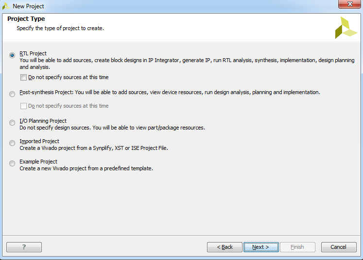
Figure 4 Vivado “New Project Type” window for RTL design entry
Add Source files in Vivado Project
By clicking next on the “Project Type” window in Figure 4 Vivado will open a new “Add source” window as in Figure 5
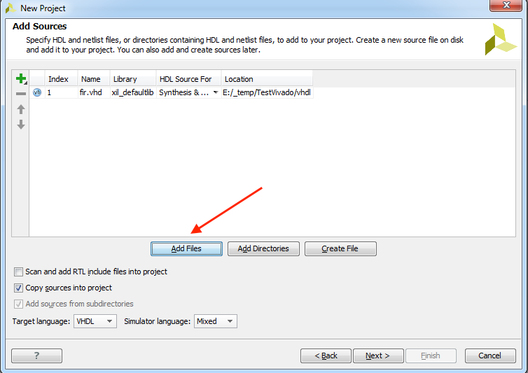
Figure 5 Vivado Add Source window
On the “Add Source” window we can add:
- A single/multiple VHDL (or other HDL files)
- A directory containing RTL design files
- Create a VHDL (or other HDL) source file using the embedded text editor
The next window is related to the IPs. In the “Add existing IP” of Figure 6 we can add an existing IP in our design. An IP can be a FIFO, a DDR memory controller, a ROM, dual-port RAM, in other words, any component targeted for the current FPGA and instantiated inside our VHDL design. The “Add existing IP” function is optional. If you don’t need any additional IP you can skip this window by clicking next.
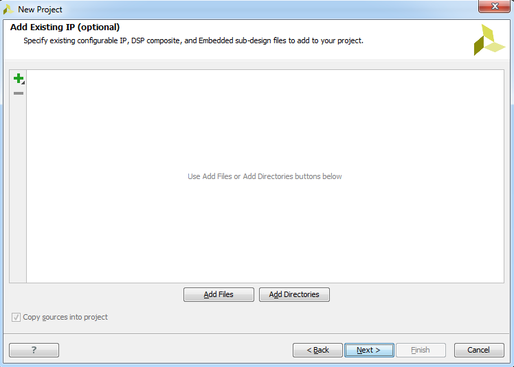
Figure 6 Vivado Add Existing IP
The next window is related to the “Add Constraint” function as in
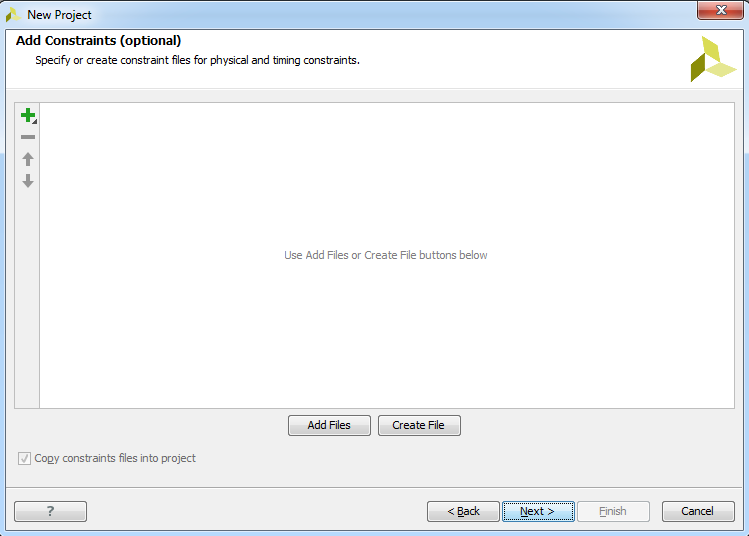
Figure 7 Vivado Add Constraint window
Every design should have a constraint file. The constraint files are related mainly to
- Timing
- Mapping, when you need to fix a location of your design inside the FPGA
- Pin
In the first run of your design, you can skip this step and complete the design to understand is the design flow works fine. You can create and add the design constraint file in a second step after the first trial layout. In this case, you can use the Vivado GUI to create and add design constraints.
Notice that, if you don’t set timing constraints Vivado does not provide the timing analysis.
Vivado Project Part selection
The last step to create a project on Vivado is the Device selection of Figure 8.
In this window, you can select the FPGA device you need to use for your design when “Part” is selected. If you select the tab “Boards”, as in Figure 9, you can enter the Xilinx board you want to use. In this case, Vivado set up the project using the pin constraint for the FPGA to match with the selected board.
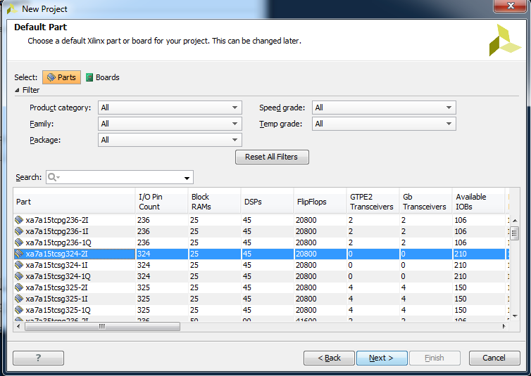
Figure 8 Vivado project device selection
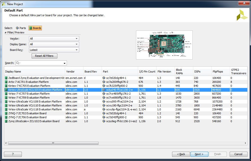
Figure 9 Vivado project board selection
The last window reports the project summary as in
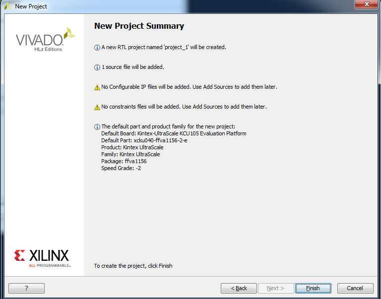
Figure 10 Vivado New Project Summary window
Vivado Run Project Implementation
By clicking finish, Vivado initializes the project and is ready to start compiling the VHDL design.
To start compiling the design just click on the “play” button as in Figure 11
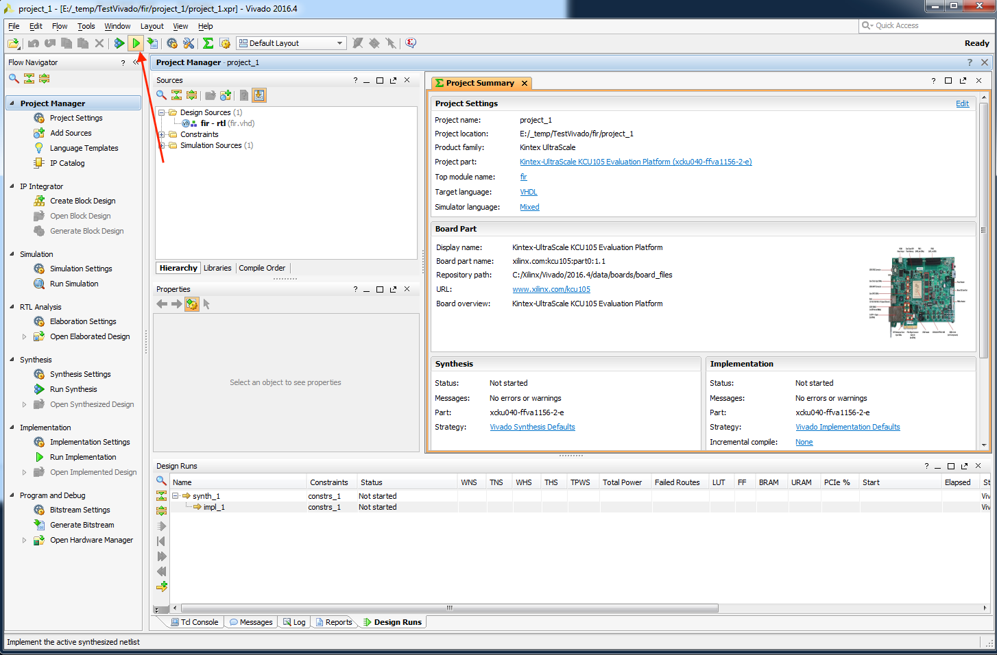
Figure 11 Run implementation design in Vivado
Conclusion
This post reports how to create a project on Vivado including the VHDL design files. The step to follow for design implementation are summarized below:
- Click “Create New Project” on the main page
- Set “Project Name” and “Project Location”
- Select the type of project
- Add Source Files
- Add existing IP (if any)
- Add constraint file
- Select FPGA or Board
- Run implementation
Ok, everything is ready to start a new design using Xilinx Vivado
Reference
[2] https://www.xilinx.com/products/design-tools/vivado.html
Tell me more!