Connecting two devices
When we need to transfer data from two different devices, the simple way is to use the minimum numbers of wires. For instance, if we need to transfer a data bus of 16 bits between two different FPGA at a rate of 1 MHz, we need to connect at least
16-bit data + 1 bit enable + 1 bit clock = 18 wires running @ 1 MHz. As you can see, these are a lot of wires! Moreover, a skew between the bits in the parallel data bus can affect the connection integrity.
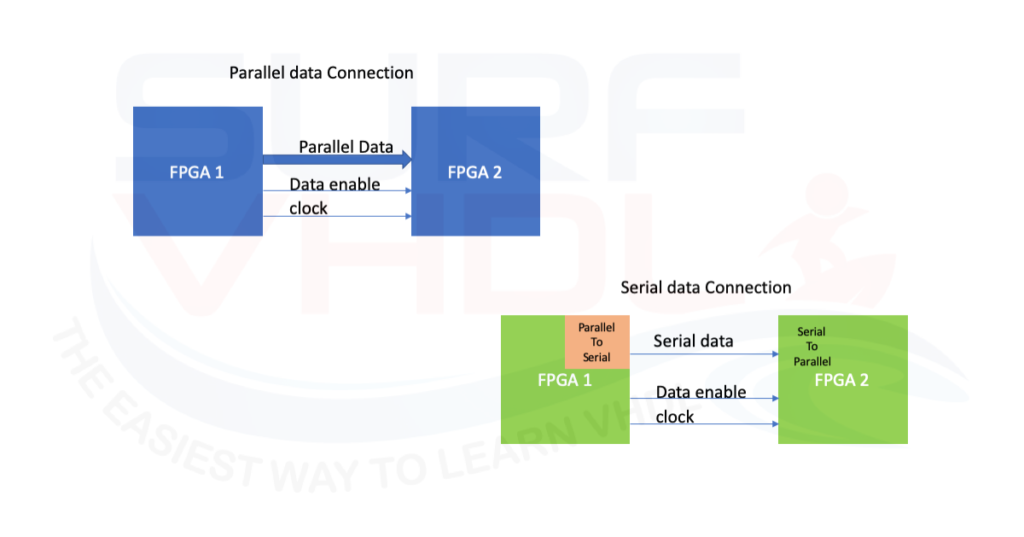
Another method for data transfer, could be to serialize the parallel data using less connection.
In this case the 16 bits will be serialized in a single bit data stream. Of course, if you need to guarantee the same data rate you need to use a higher speed in data transfer.
If you need to transfer 16-bit data @ 1MHz the serial data stream speed shall be at least greater than 16 x 1 MHz = 16 MHz.
Parallel to Serial converter VHDL code example
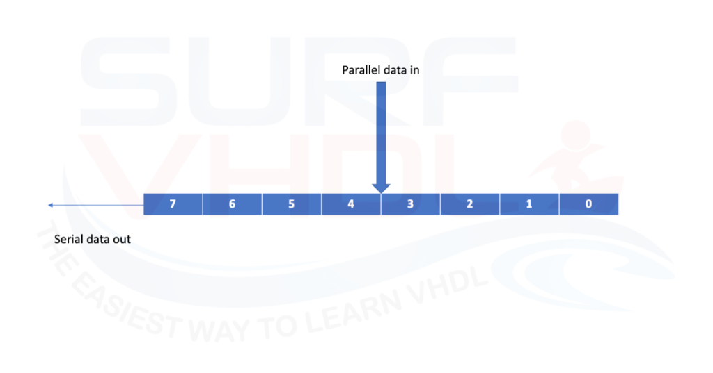
Let assume the parallel data bus of the Parallel to Serial converter to be N bit. The parallel input to the module shall be at a rate of less than or equal to 1/N clock cycles. The serializer section takes N clock cycles to output the serial data stream.
An example of Parallel to Serial converter VHDL code is given below:
library ieee;
use ieee.std_logic_1164.all;

entity parallel2serial is
generic(
	G_N               : integer:=8 );
port (
	i_clk                          : in  std_logic;
	i_rstb                         : in  std_logic;
	i_data_ena                     : in  std_logic;
	i_data                         : in  std_logic_vector(G_N-1 downto 0);
	o_data_valid                   : out std_logic;
	o_data                         : out std_logic;
	o_error_serialize_pulse        : out std_logic);
end parallel2serial;

architecture rtl of parallel2serial is
signal r_data_enable                  : std_logic;
signal r_data                         : std_logic_vector(G_N-1 downto 0);
signal r_count     : integer range 0 to G_N;

begin
o_data_valid    <= r_data_enable;
o_data          <= r_data(G_N-1);

p_paralle2serial : process(i_clk,i_rstb)
begin
	if(i_rstb='0') then
		r_count              <= G_N-1;
		r_data_enable        <= '0';
		r_data               <= (others=>'0');
		o_error_serialize_pulse    <= '0';
	elsif(rising_edge(i_clk)) then
		if(r_count<G_N-1) and (i_data_ena='1') then
			o_error_serialize_pulse    <= '1';
		else
			o_error_serialize_pulse    <= '0';
		end if;
		if(i_data_ena='1') then
			r_count        <= 0;
			r_data_enable  <= '1';
			r_data         <= i_data;
		elsif(r_count<G_N-1) then
			r_count        <= r_count + 1;
			r_data_enable  <= '1';
			r_data         <= r_data(G_N-2 downto 0)&'0';
		else
			r_data_enable  <= '0';
		end if;
	end if;
end process p_paralle2serial;

end rtl;
In the VHDL code is implemented an error detection logic. The error detection logic rises the “o_error_serialize_pulse” if the input data enable is high during the serialization process. I mean, if the parallel data is not yet totally serialized, no other input data can be processed.
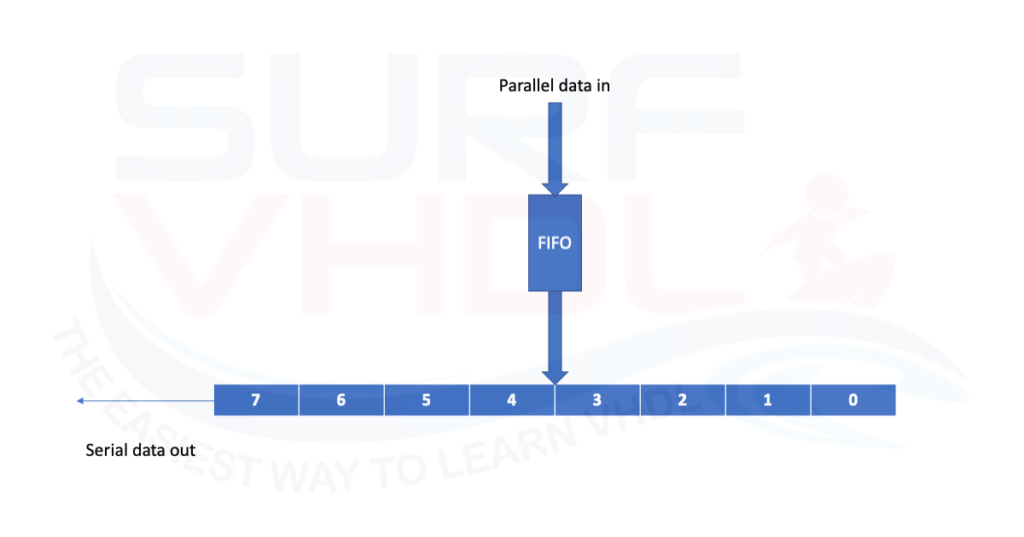
If you need to handle different input timing you can implement a simple input FIFO logic in order to buffer the incoming parallel data. The read fifo logic will enable the read fifo data each 1/N clock cycles.
It is clear that the FIFO depth shall be sized depending on the input data timing and, in any cases, the input data rate shall be less than or, at least, equal to the output serial data rate as in equation EQ1
ParallelDataRate <= SerialDataRate * N EQ1
Parallel to serial converter VHDL simulation results
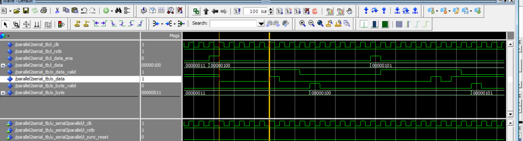
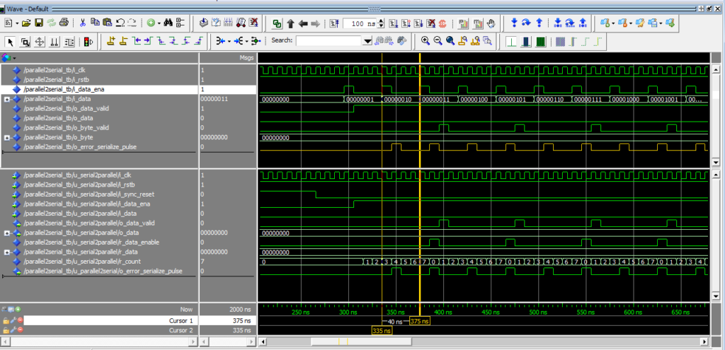
In the simulation of all the figures below, the clock is set to 10 ns, so 80 ns mean 8 clock cycles.
In Figure4 is reported a simulation of the parallel to serial converter VHDL code above. First serial output bit is the MSB of the input parallel data. You can choose to output first the LSB. It depends on the convention you are using. In the
In is reported an overview of the parallel to serial converter VHDL code. As clear the input byte to be serialized is re-parallelized in the byte signal.
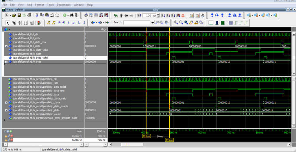
In Figure 5 is highlighted the ZOOM-IN of the serial conversion of the parallel pattern “00000100”. As clear after 5 clock cycle of “o_data” equal to zero, the signal goes to one for one clock cycle, then to zero for the last two clock cycles.
Reports an example of serialization error. In this case the input data enable occurs every 40 ns, i.e. every 4 clock cycles
Conclusion
In this post, we implemented a simple example of parallel to serial VHDL code. Such a conversion strategy can be used when we need to connect two different devices like two FPGA and we need to minimize the connection wires. The clock for the data connection must run at least N times faster (where N is the number of bits to serialize).
Using a serial connection, we can minimize the number of connection wires, minimizing also the skew problem on the connection itself.
Good Evening, we working our final year project at VLSI domain.we need help for coding .TITLE:wireless data transmission betwwen two fpga
Regarding about test bench