How To Implement Clock Divider in VHDL

Clock Design Overview

Often, inside our FPGA design, we have the necessity to generate a local clock from the system clock. With system clock, I mean the clock that is coming from an external board oscillator. Many modern FPGAs have the possibility to generate internal clocks, different from the external clocks, using internal PLL hard macro. So you can generate internal FPGA clock as multiple or sub-multiple of the external system clock.
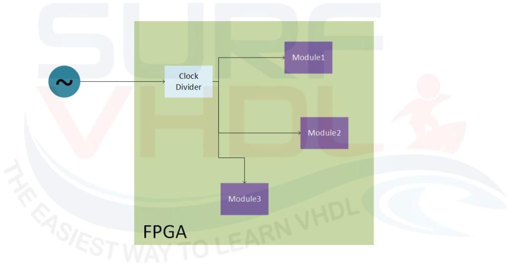
 

Figure1 - FPGA with internal clock divider
Figure1 – FPGA with internal clock divider

Sometimes the PLL are used to modify the clock phase or to generate different clocks at the same frequency with different phase relationship. For instance, 3 clocks:

Read More

What is a FIFO?

Basic notion on FIFO (First-In First-Out)

FIFO means First-In First-Out. A FIFO is a structure used in hardware or software application when you need to buffer a data.
Basically, you can think about a FIFO as a bus queue in London.
The people that arrive first is the one who catch the bus first….

FIFO example at bus Stop
Figure1 – FIFO example at bus Stop

Of course, this example is valid only in London or in Japan, in other countries, it could be not be used 🙂 Read More

How to Implement a Digital Delay Using a Dual Port Ram

Implement a Digital Delay Using a Dual Port Ram

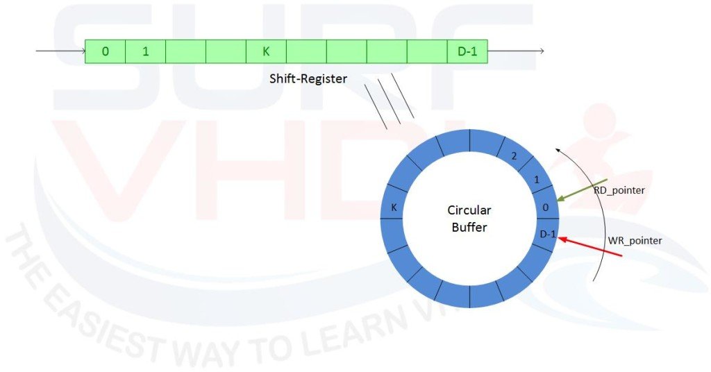
The digital delay lines are one of the most used blocks in the digital design. When the digital delay is small in terms of numbers of Flip-Flop a simple shift register approach can be used. If the number of bits to delay i.e. the number of Flip-Flop utilized became important, a different approach should be used.

Digital Delay Implementation Architecture as Circular Buffer
Figure 1 – Digital Delay Implementation Architecture as Circular Buffer 

In this post, a FIFO delay approach has been presented. In that case, we used the FIFO macro provided by the FPGA vendor in order to implement a digital delay line.

Read More

How To Generate Sine Samples in VHDL

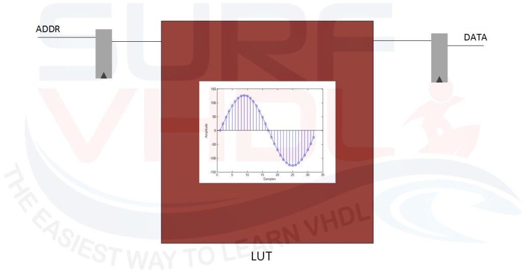
In Digital Signal Processing, often is required the implementation of transcendental math function as trigonometric functions (sine, cosine, tan, atan) or exponential and logarithmic functions and so on. An efficient way, when possible, is to implement an approximation of these functions using Look Up Table or LUT as the sine example in Figure1.

Figure1 - LUT implementing sine function
Figure1 – LUT implementing sine function


In modern FPGA a large amount of RAM/ROM memory is available, so the LUT implementation requires only FPGA memory hardware resources and few additive registers. Read More

How To Implement Shift-Register in VHDL Using a FIFO

How To Implement Shift-Register in VHDL Using a FIFO

When you implement a digital design one of the most used building block is a pipeline or a digital delay line. For instance, you could need to compensate the delay between two

For instance, you could need to compensate the delay between two branches of  a digital circuit in terms of clock cycle. In

In Figure1, there is a possible example where you have to subtract the value of an input sample of an ADC and this value is computed using the ADC sample as well. In the figure, the “Processing Block” compute the required functions over the current ADC samples. Then the correction has to be subtracted to the current ADC input samples. So you need to compensate the processing time in terms of clock cycle using a feed-forward architecture implemented as a delay line.

Figure1 – An example of digital delay line requirement


Read More

Write to File in VHDL using TextIO Library

Write to File in VHDL using TextIO Library

When you simulate a design in VHDL it is very useful to have the possibility to save some simulation results. For example, if you need to compare the simulation results with reference test vector, or simply to document the simulation in a test report.

Write File Test Bench Architecture

In VHDL, there are predefined libraries that allow the user to write to an output ASCII file in a simple way. The TextIO library is a standard library that provides all the procedure to read from or write to a file. Read More

Read from File in VHDL using TextIO Library

Read from File in VHDL using TextIO Library

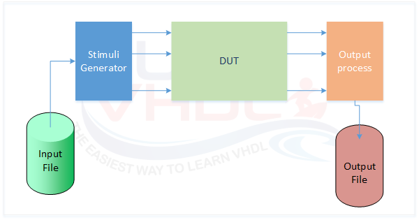
When you need to simulate a design in VHDL it is very useful to have the possibility to read the stimuli to provide to your Design Under Test (DUT) reading from an input file.

This approach allows you to have different test bench input stimuli using the same VHDL test bench code.

Read from file in VHDL and generate test bench stimuli

In VHDL, there are predefined libraries that allow the user to read from an input ASCII file in a simple way. Read More

How to Implement a Finite State Machine in VHDL

What is a Finite State Machine or FSM?

Which can be an effective and elegant way to describe a control logic? Which strategies would you use?

One possibility is trivial: start writing your control logic with a series of “if then else” or “case” statement.

Definitely, not an elegant method but in some ways could perhaps be efficient if you are particularly skilled at simplifying the description of your control logic.

Another possibility is to use a Finite State Machine (FSM). Read More

How to Design SPI Controller in VHDL

Serial Peripheral Interface Introduction

Before reading the post, if you need the VHDL code of the SPI controller, just put your email in the box you find in the post. There is no need to post a comment asking me for the code 🙂 If you don’t receive the email, please check your SPAM folder, enjoy!

The Serial Peripheral Interface (SPI) bus is a synchronous serial communication controller specification used for short-distance communication, primarily in embedded systems. The interface was developed by Motorola and has become a de-facto standard. Typical applications include sensors, Secure Digital cards, and liquid crystal displays.

SPI devices communicate in full-duplex mode using a master-slave architecture with a single master. The SPI master device originates from the frame for reading and writing. Multiple SPI slave devices are supported through selection with individual slave select (SS) lines as in Figure 2.

Figure 1 - SPI Master-single slave
Figure 1 – SPI Master-single slave

Read More

How to Implement FIR Filter in VHDL

FIR Filter Introduction

Finite Impulse Response (FIR) filters are characterized by a time response depending only on a given number of the last samples of the input signal. For a causal discrete-time FIR filter of order N, each value of the output sequence is a weighted sum of the most recent input values:


fir_filter_equation


where:

  • x[n] is the input signal,
  • y[n] is the output signal,
  • N is the filter order; a Nth-order filter has (N+1) terms on the right-hand side
  • bi is the value of the impulse response at the i’th instant for 0<= i <=N of a Nth-order FIR filter. If the filter is a direct form FIR filter then is also a coefficient of the filter (see Figure1).

Read More