Clock Design Overview
Often, inside our FPGA design, we have the necessity to generate a local clock from the system clock. With system clock, I mean the clock that is coming from an external board oscillator. Many modern FPGAs have the possibility to generate internal clocks, different from the external clocks, using internal PLL hard macro. So you can generate internal FPGA clock as multiple or sub-multiple of the external system clock.
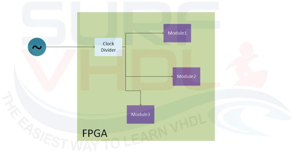
Sometimes the PLL are used to modify the clock phase or to generate different clocks at the same frequency with different phase relationship. For instance, 3 clocks:
Clock1, clock2 and clock3 where:
- Clock1 is the reference clock
- Clock2 has 90° phase offset
- Clock3 has 180° phase offset
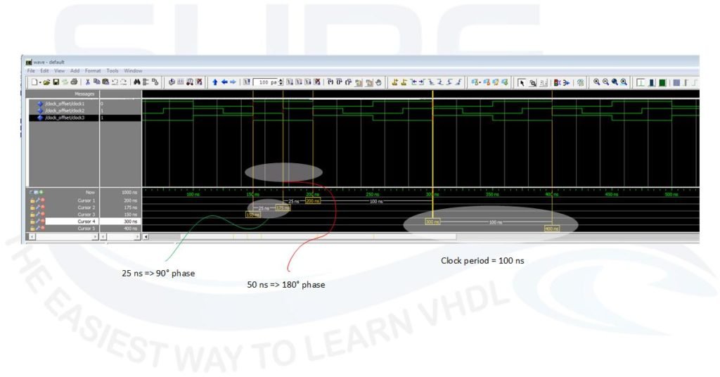
- Clock1 has a 100 ns period.
- Clock2 offset with respect to clock1 is 25 ns = 100 ns/4 (i.e. 90° ).
- Clock3 offset with respect to clock1 is 50 ns = 100 ns/2 (i.e. 180° ).
Clock division by two
If the clock we need is simply the system clock divided by two, we can implement a simple divider using a flip-flop and inverter:

This is the simplest clock divider you can implement into an FPGA or ASIC. Sometimes this approach is used to generate a clock with 50% duty cycle even starting from a source clock that has a duty cycle different from 50%
Figure4 show an example where the source clock has duty cycle 34/66 and the divided clock has a duty cycle of 50%

The VHDL code for a clock divider by 2 is:
signal clk34_66       : std_logic:='0';
signal clk_div2       : std_logic:='0';

begin

-- test clock generator
-- NOT synthesizable only for test
p_clk34_66 : process
begin
  clk34_66  <= '0';
  wait for 34 ns;
  clk34_66  <= '1';
  wait for 66 ns;
end process p_clk34_66;

-- divider by two: synthesizable VHDL code
p_clk_div2: process(clk34_66)
begin
  if(rising_edge(clk34_66)) then
    clk_div2   <= not clk_div2;
  end if;
end process p_clk_div2;
As you can see is a simple process that implements the flip-flop and inverter of Figure3.
Clock division by power of two
If you generalize the clock divider by two, a smart and efficient divider is the clock divider by a power of two. This clock divider can be implemented using a free running simple wrap around counter as in Figure5.
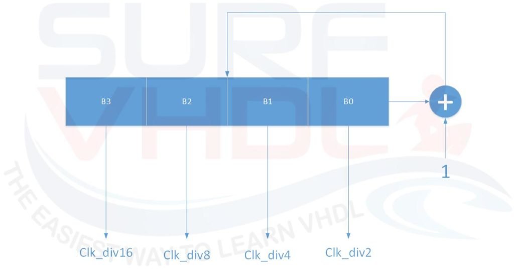
You can think about at the clock divider by two, as a wraparound counter where the Least Significant Bit (LSB) is used to generate the clock. The counter LSB flips at half the clock rate, this means that it can be used as clock divider by two.
What happen to the others bit?
The second bit, bit1, numbering LSB as bit 0, change its status at half of bit 0, so bit 1 rate is ¼ of clock rate. The bit k rate is 1/(2^(k+1)) clock rate.
For instance, bit 3 rate is
1/(2^(3+1)) = 1/16
The VHDL for clock divider by a power of two is very simple and straightforward as you can see in the example below.
library IEEE;
use IEEE.std_logic_1164.all;
use IEEE.numeric_std.all;

entity clock_div_pow2 is
port(
  i_clk         : in  std_logic;
  i_rst         : in  std_logic;
  o_clk_div2    : out std_logic;
  o_clk_div4    : out std_logic;
  o_clk_div8    : out std_logic;
  o_clk_div16   : out std_logic);
end clock_div_pow2;

architecture rtl of clock_div_pow2 is

signal clk_divider        : unsigned(3 downto 0);

begin


p_clk_divider: process(i_rst,i_clk)
begin
  if(i_rst='0') then
    clk_divider   <= (others=>'0');
  elsif(rising_edge(i_clk)) then
    clk_divider   <= clk_divider + 1;
  end if;
end process p_clk_divider;

o_clk_div2    <= clk_divider(0);
o_clk_div4    <= clk_divider(1);
o_clk_div8    <= clk_divider(2);
o_clk_div16   <= clk_divider(3);

end rtl;
In this VHDL code of the clock divider, we have introduced the asynchronous reset signal.
If you do not reset the clk_counter at a known state, the simulation doesn’t run.
It is a good design rule to reset the clock divider unless differently specified because you will start your clock divider state from a known condition. Implementing the divider without the reset signal, you shall set the initial condition to clk_counter signal during the declaration of the signal itself:
signal clk_counter : unsigned(3 downto 0):=(others=>'0');
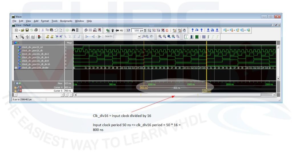
Remember that this VHDL code it is still synthesizable, so you can use it without any problem, but your clock divider start condition is unknown. The simulation of the VHDL code for the clock divider by power of two is reported in Figure6
Clock division by an integer
What if you need a derived clock that is an integer submultiple of your board clock?
Can we generalize the approach we saw above?
The answer is YES.
If we need a derived clock that is an integer submultiple of the source clock, we can still use a counter to divide the source clock, just counting how long the derived clock shall stay high and how long the derived clock shall stay low. Of course, when we state “how long”, this time, is given in terms of source clock cycles.
A possible VHDL code implementation of an integer clock divider is given below.
library IEEE;
use IEEE.std_logic_1164.all;
use IEEE.numeric_std.all;

entity clock_div is
port(
  i_clk         : in  std_logic;
  i_rst         : in  std_logic;
  i_clk_divider : in  std_logic_vector(3 downto 0);
  o_clk         : out std_logic);
end clock_div;

architecture rtl of clock_div is

signal r_clk_counter        : unsigned(3 downto 0);
signal r_clk_divider        : unsigned(3 downto 0);
signal r_clk_divider_half   : unsigned(3 downto 0);

begin

p_clk_divider: process(i_rst,i_clk)
begin
  if(i_rst='0') then
    r_clk_counter       <= (others=>'0');
    r_clk_divider       <= (others=>'0');
    r_clk_divider_half  <= (others=>'0');
    o_clk               <= '0';
  elsif(rising_edge(i_clk)) then
    r_clk_divider       <= unsigned(i_clk_divider)-1;
    r_clk_divider_half  <= unsigned('0'&i_clk_divider(3 downto 1)); -- half
    if(r_clk_counter < r_clk_divider_half) then
      r_clk_counter   <= r_clk_counter + 1;
      o_clk           <= '0';
    elsif(r_clk_counter = r_clk_divider) then
      r_clk_counter   <= (others=>'0');
      o_clk           <= '1';
    else
      r_clk_counter   <= r_clk_counter + 1;
      o_clk           <= '1';
    end if;
  end if;
end process p_clk_divider;

end rtl;
In the VHDL example, the counter is used to count the number of source clock cycles we want the derived clock to stay high and stay low. As you can see the clock division factor “clk_div_module” is defined as an input port. The generated clock stays high for half “clk_div_module” cycles and low for half “clk_div_module“.
- If “clk_div_module” is even, the clock divider provides a divided clock with 50% duty cycle.
- If “clk_div_module” is odd the duty cycle cannot be 50%.
In case “clk_div_module” is odd, the duty cycle approaches 50% for high division factor. For instance
"clk_div_module" = 3; clock high = 2 cycle; clock low = 1 cycles; duty ~33/66

"clk_div_module" = 15; clock high = 8 cycle; clock low = 7 cycles; duty ~46/54

"clk_div_module" = 6; clock high = 3 cycle; clock low = 3 cycles; duty 50/50

Clock tree handling
This post received a lot of comment either in the social channels and on this website. Many of these considerations are founded since in the post no clarification on how to handle the clock tree has been done.
So let’ clarify better this point. When you use this kind of approach you must pay attention on how the layout tool “understands” this architecture, I mean, you must check if the layout tool inserts clock buffer on the root of your clock.
Generally, the layout tool as ISE or Quartus are smart enough and insert automatically the clock buffers on the root of the clock tree, i.e at the output of the clock divider module. You have to check if these buffers are present and provide the tool with the proper timing constraints. If no buffers are inserted, you must insert by hand in order to not destroy the timing performance of your design.
VHDL Clock divider design example
In order to clarify better for the people that are still skeptical, let’s implement a simple design of the FIR architecture discussed in this post “How to Implement FIR Filter in VHDL” . These two implementations will be tested on ALTERA Cyclone III “EP3C16F484C6” present in the DE0 ALTERA board:
- Implement the filter using the clock provided by the dedicated pin of the FPGA as in Figure8
- Using a divided clock, by mean of the clock divider above as in Figure9.


The VHDL code for the simple implantation of Figure8 is presented below. In this case, the FPGA entity “fir_filter_pad” is a simple wrapper for the component “fir_filter_4”.
library ieee;
use ieee.std_logic_1164.all;
use ieee.numeric_std.all;

entity fir_filter_pad is
port (
  i_clk        : in  std_logic;
  i_rstb       : in  std_logic;
  -- coefficient
  i_coeff_0    : in  std_logic_vector( 7 downto 0);
  i_coeff_1    : in  std_logic_vector( 7 downto 0);
  i_coeff_2    : in  std_logic_vector( 7 downto 0);
  i_coeff_3    : in  std_logic_vector( 7 downto 0);
  -- data input
  i_data       : in  std_logic_vector( 7 downto 0);
  -- filtered data
  o_data       : out std_logic_vector( 9 downto 0));
end fir_filter_pad;

architecture rtl of fir_filter_pad is

component fir_filter_4
port (
  i_clk        : in  std_logic;
  i_rstb       : in  std_logic;
  -- coefficient
  i_coeff_0    : in  std_logic_vector( 7 downto 0);
  i_coeff_1    : in  std_logic_vector( 7 downto 0);
  i_coeff_2    : in  std_logic_vector( 7 downto 0);
  i_coeff_3    : in  std_logic_vector( 7 downto 0);
  -- data input
  i_data       : in  std_logic_vector( 7 downto 0);
  -- filtered data
  o_data       : out std_logic_vector( 9 downto 0));
end component;

begin

u_fir_filter_4 : fir_filter_4
port map(
  i_clk        => i_clk        ,
  i_rstb       => i_rstb       ,
  -- coefficient
  i_coeff_0    => i_coeff_0    ,
  i_coeff_1    => i_coeff_1    ,
  i_coeff_2    => i_coeff_2    ,
  i_coeff_3    => i_coeff_3    ,
  -- data input
  i_data       => i_data       ,
  -- filtered data
  o_data       => o_data       );

end rtl;
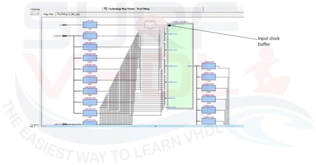
The layout of this code produces the implementation of Figure10 where it is clear that the “fir_filter_pad” is only a wrapper where the only add-ons are the PAD buffer and the global clock buffer.
In the second example the FPGA container “fir_filter_clock_div_pad” instantiates two components:
- The FIR filter
- The clock divider
library ieee;
use ieee.std_logic_1164.all;
use ieee.numeric_std.all;

entity fir_filter_clock_div_pad is
port (
  i_clk         : in  std_logic;
  i_rstb        : in  std_logic;
  i_clk_divider : in  std_logic_vector(3 downto 0);
  -- coefficient
  i_coeff_0     : in  std_logic_vector( 7 downto 0);
  i_coeff_1     : in  std_logic_vector( 7 downto 0);
  i_coeff_2     : in  std_logic_vector( 7 downto 0);
  i_coeff_3     : in  std_logic_vector( 7 downto 0);
  -- data input
  i_data        : in  std_logic_vector( 7 downto 0);
  -- filtered data
  o_data        : out std_logic_vector( 9 downto 0));
end fir_filter_clock_div_pad;

architecture rtl of fir_filter_clock_div_pad is

component clock_div
port(
  i_clk         : in  std_logic;
  i_rst         : in  std_logic;
  i_clk_divider : in  std_logic_vector(3 downto 0);
  o_clk         : out std_logic);
end component;

component fir_filter_4
port (
  i_clk        : in  std_logic;
  i_rstb       : in  std_logic;
  -- coefficient
  i_coeff_0    : in  std_logic_vector( 7 downto 0);
  i_coeff_1    : in  std_logic_vector( 7 downto 0);
  i_coeff_2    : in  std_logic_vector( 7 downto 0);
  i_coeff_3    : in  std_logic_vector( 7 downto 0);
  -- data input
  i_data       : in  std_logic_vector( 7 downto 0);
  -- filtered data
  o_data       : out std_logic_vector( 9 downto 0));
end component;

signal w_clk_div        : std_logic;

begin

u_clock_div : clock_div
port map(
  i_clk         => i_clk         ,
  i_rst         => i_rstb        ,
  i_clk_divider => i_clk_divider ,
  o_clk         => w_clk_div     );

u_fir_filter_4 : fir_filter_4
port map(
  i_clk        => w_clk_div    ,
  i_rstb       => i_rstb       ,
  -- coefficient
  i_coeff_0    => i_coeff_0    ,
  i_coeff_1    => i_coeff_1    ,
  i_coeff_2    => i_coeff_2    ,
  i_coeff_3    => i_coeff_3    ,
  -- data input
  i_data       => i_data       ,
  -- filtered data
  o_data       => o_data       );

end rtl;
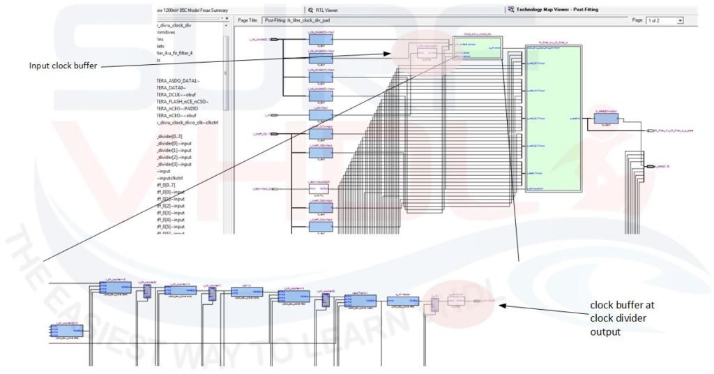
Layouting this code, the MAP viewer highlight the presence of the two component FIR and clock divider plus the global input clock and PAD. Going down in the hierarchy a second clock buffer, highlighted in Figure11 is present. Quartus recognize that the clock generated by the process inside the “clock_div” module is a clock used in the design, so provides to add automatically the clock buffer. Note that the clock buffer is present inside the module clock_div.
In order to compare if the insertion of the module clock divider corrupts the timing performances of the design, let’s check the design report of Figure12
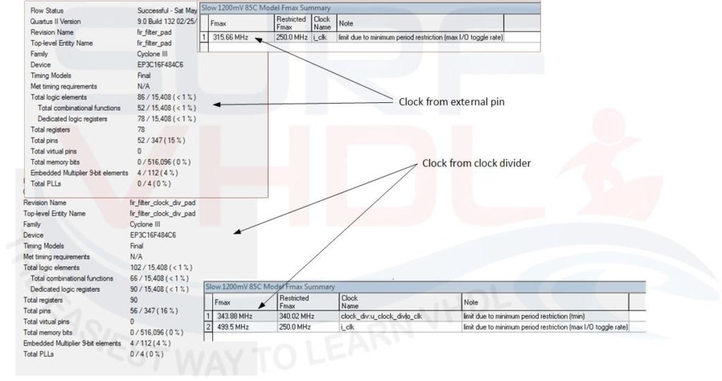
As clear the design with the “discrete” clock divider is in line with the timing performances of the design taking the clock from the dedicated pin, moreover, the design with clock divider has slightly better performances!
Final consideration on integer clock division on FPGA
We demonstrate that using an integer clock divider the VHDL design maintains the same timing performances of a design with the clock provided on a dedicated clock pin. This approach can be used when you need to divide by integer your clock and you don’t have the possibility or don’t want to instantiate a PLL/DCM inside the FPGA.
A good reason for using this approach could be if you need to change “run-time” the clock division factor, for instance, to slow down the clock when you need to save power consumption. The integer clock divider allows you to reconfigure the clock frequency simply setting the clock division factor.
When you deal with custom hard macro inside the FPGA i.e transceiver, PCIe macro and so on, this approach cannot be used. In this case, the layout tool raises an error when the clock routing is not possible.
You can use the code above for your VHDL clock design if you need a clock divider by an integer in your design without using the FPGA PLL/DCM.
If you use VHDL / RTL code for your clock divider you can easily port your VHDL code on different FPGA or ASIC technology. Using PLL approach you need to tailor your code on different technology.
If you appreciated this post, please help us to share it with your friend.
[social_sharing style=”style-7″ fb_like_url=” https://surf-vhdl.com/how-to-implement-clock-divider-vhdl” fb_color=”light” fb_lang=”en_US” fb_text=”like” fb_button_text=”Share” tw_lang=”en” tw_url=” https://surf-vhdl.com/how-to-implement-clock-divider-vhdl” tw_button_text=”Share” g_url=” https://surf-vhdl.com/how-to-implement-clock-divider-vhdl” g_lang=”en-GB” g_button_text=”Share” linkedin_url=” https://surf-vhdl.com/how-to-implement-clock-divider-vhdl” linkedin_lang=”en_US” alignment=”center”]
If you need to contact us, please write to surf.vhdl@gmail.com
We appreciate any of your comment, please post below:
And now fractional clock dividers
In a next post relative to NCO, it will be possible to generate a fractional clock. In this case, you may have a jitter in the clock generation
how to modify the code if we want to just divide by an interger say, 5 , of a 50Mhz source clock.
just set “i_clk_divider” to 5 = “0101” and put the 50MHz clock as input clock
Hi,
I was trying to understand the clock_div by integer code to get a 10MHz clock from a 50 MHz source clock.
As, mentioned i made the changes at the input.
i_clk_divider : in std_logic_vector:=”0101″;
Can you please guide me the changes below to get the 10Mhz clock. (I get error 10485. range direction of object must be same as range direction of object.
r_clk_divider_half <= unsigned('0'&i_clk_divider(3 downto 1)); — half
if(r_clk_counter < r_clk_divider_half) then
r_clk_counter <= r_clk_counter + 1;
o_clk <= '0';
elsif(r_clk_counter = r_clk_divider) then
r_clk_counter ‘0’);
o_clk <= '1';
else
r_clk_counter <= r_clk_counter + 1;
o_clk <= '1';
end if;
end if;
end process p_clk_divider;
end rtl;
The entity “clock_div” should be instantiated as a component in your VHDL design.
When you will instantiate the component you have to set the input port
“i_clk_divider : in std_logic_vector(3 downto 0);”
with the value 5 because you need to divide your 50MHz clock by 5 to get the 10 MHz clock.
for instance:
clk_divider <= "0101"; and then map to the port You don't need to modify the entity, just set the proper value to the input port during the instantiation. you can take a look to get an example of component instantiation http://surf-vhdl.com/vhdl-syntax-web-course-surf-vhdl/vhdl-structural-modeling-style/
Hi,
I have made the component instantiate as follows. I get the error as “near text begin ; expecting entity , or architecture or use or library(10500) . I feel that the program is correct. Can you please point the possible mistake.
component clock_div
port(
i_clk_divider : “0101”
);
end component;
begin
comp_inst:clock_div
port map(i_clk_divider <="0101");
end;
begin
p_clk_divider: process(i_rst,i_clk)
begin
if(i_rst='0') then
r_clk_counter ‘0’);
r_clk_divider ‘0’);
r_clk_divider_half ‘0’);
o_clk <= '0';
elsif(rising_edge(i_clk)) then
r_clk_divider <= unsigned(i_clk_divider)-1;
r_clk_divider_half <= unsigned('0'&i_clk_divider(3 downto 1)); — half
if(r_clk_counter < r_clk_divider_half) then
r_clk_counter <= r_clk_counter + 1;
o_clk <= '0';
elsif(r_clk_counter = r_clk_divider) then
r_clk_counter ‘0’);
o_clk <= '1';
else
r_clk_counter <= r_clk_counter + 1;
o_clk <= '1';
end if;
end if;
end process p_clk_divider;
end rtl;
Dear SUNIL,
the component instantiation you’ve made is wrong.
You can refresh the component instantiation concept in the “VHDL Syntax” section
http://surf-vhdl.com/vhdl-syntax-web-course-surf-vhdl/
or if you prefer you can join the Udemy course from this link
https://surf-vhdl.teachable.com
None of these approaches are suitable for use in an FPGA, since they result in the divided clock signals appearing on regular routing buses in the logic fabric instead of the special high speed clock buses. You only want clocks on the dedicated global clock signals, otherwise you could end up with horrendous skew between different parts of your circuit. If you want a divided clock in an FPGA, you should stick to using the PLL/DCM components in the clock management tiles.
jadwin79,
thank you for your feedback.
You are right if you talk about of very old FPGA and if you don’t use the global clock network.
After clock division, you need to “connect” the divided clock to the global clock tree.
Generally, the layout tool recognizes the clock and put a clock global buffer to drive the high fan-out clock network.
You need to check if the tool has instantiated the global clock buffer.
If not, you need to add it by hand.
The best way to do this is to create a component where you will handle all the clocks present in your design. With this approach, you can control in an efficient way the clock tree of your design.
Quartus II is very smart and adds automatically the global buffer to every signal with high fanout. If you check on the fitter report, you can verify that Quartus adds the global buffer hard macro on the clock, reset and the others high fanout netlist.
ISE / VIVADO, generally add automatically clock buffers but sometimes fails.
You shall check the timing and area report to verify that the tool correctly “understands” your design. It is only a software!
Another consideration is that you are dividing a clock, so the minimum division is by two. This means that you are running at half of your reference clock.
Last consideration.
We used and continue to use this approach in complex design, for example, a high-speed modem with different clock domains where some of these clock domains are derived by integer division from the main clock. Even using this approach the section of the design driven by divided clock runs up to 200 MHz on a Stratix IV with area occupation of 80%.
As Long as you do not do any mistakes in your hdl description or have ambiguities, the Tools are intelligent and instantiates clk buffers! The last 15 years I had no Problems!
Hi all,
I agree with jadwin79.
In my humble opinion, synthesis and implementation of a vhdl project, with different clock domains, using non global clocks buses can produce high undesirable skew values.
I use a similar approach presented in this discussion. We use a counter with a comparator to generate a signal with a lower frequency than the system clock. However, it is used as an enable signal instead of a clock signal for the components and process that need working with lower frequency than the system clock. With this technique all the design uses a single clock routed to the global clock buses using clock enables to work at lower frequencies.
Is someone using this kind of technique? I thought it is very extended procedure.
Hi Marcos,
you can use a “discrete” clock divider without any problem.
In order to explain better and clarify that no issue are present using this approach, I updated the post inserting an example that demonstrates the functionality.
Functionality isn’t the issue, it’s skew and the possibility of glitches.
Your approach doesn’t control for either of these. If the circuit is simple, you may get close to the correct result. More than likely, the tool will place all the combinatorial logic before the registers, but you can’t be sure of that.
Now, you _can_ use this sort of approach properly in FPGA or ASIC, but you would want to make sure 1, that the output is really registered and it didn’t decide to make (say) a ripple carry counter, 2, that any sort of glitch is filtered by at at least one more set of flops and 3, constraints are added to make sure that the APR tools know what skew is acceptable.
There is a reason that dedicated clock buffer and more importantly clock gate cells exist.
Thanks for your feedback,
in the example above is clear that the output is coming from a flip-flop and the clock netlist is buffered as from the examples.
Hello Marcos,
Yes, we use clock enable signals to reduce the number of clock domains, simplify synchronisation, and simplify clock routing. I find clock enable signals more suitable and portable. The only drawback is that the design uses a higher clock frequency, but my experience is that normally I get better timing results, and normally I don’t have enough clock buffers to ensure that all the derived clocks will be routed using low jitter/skew clock networks. My company uses clock enable signals as a rule, as all the tools and devices seem to always handle them better.
Excellent article, nicely explained. Helped in building knowledge base.
Thank You for your feedback!
Thank You!
Good article. I aam dealing with some of these issus as well..
Good tutorial.. I also found this https://www.maxybyte.com/p/counter-in-vhdl-with-debouncer.html helpful
thank you