
Serial Peripheral Interface Introduction
The Serial Peripheral Interface (SPI) bus is a synchronous serial communication controller specification used for short-distance communication, primarily in embedded systems. The interface was developed by Motorola and has become a de-facto standard. Typical applications include sensors, Secure Digital cards, and liquid crystal displays.
SPI devices communicate in full-duplex mode using a master-slave architecture with a single master. The SPI master device initiates the frame for reading and writing. Multiple SPI slave devices are supported through selection with individual slave select (SS) lines as in Figure 2.
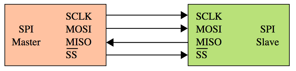
Figure 1 – SPI Master-single slave
The SPI is a four-wire serial bus as you can see in Figure 1 and in Figure 2.
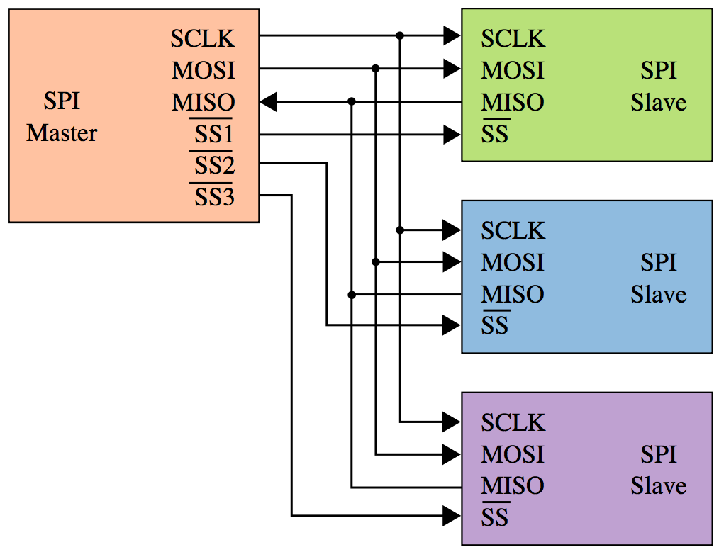
Figure 2 – SPI Master-three slaves
For further information see the Wikipedia Page dedicated to the SPI.
SPI Timing and Modes (CPOL & CPHA)
One of the most critical aspects of SPI communication is the clock configuration. The SPI protocol specifies four standard modes of operation based on two parameters: Clock Polarity (CPOL) and Clock Phase (CPHA).
- CPOL (Clock Polarity): Determines the base value (idle state) of the clock.
- CPOL = 0: Clock is low when idle.
- CPOL = 1: Clock is high when idle.
- CPHA (Clock Phase): Determines which clock edge is used to sample the data.
- CPHA = 0: Data is sampled on the first clock edge (rising or falling, depending on CPOL).
- CPHA = 1: Data is sampled on the second clock edge.
This creates four possible combinations (Mode 0 to Mode 3).
Note: The VHDL implementation provided in this article implements SPI Mode 3 (CPOL=1, CPHA=1). This means the clock idles high, data is shifted on the falling edge, and it is sampled on the rising edge.
SPI controller architecture overview
The SPI bus specifies four logic signals:
- SCLK : Serial Clock (output from master).
- MOSI : Master Output, Slave Input (output from master).
- MISO : Master Input, Slave Output (output from slave).
- SS : Slave Select (active low, output from master).
You can find alternate naming, but the functionalities are the same.
SPI timing example is shown in Figure 4. The MOSI can be clocked either on the rising or falling edge of SCLK. If MOSI changes on the rising edge of SCLK, MISO will change on the falling edge, and vice versa.
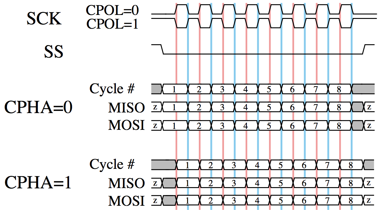
Data transmission begins on the falling edge of SS, then a number N of clock cycles will be provided. The MOSI is driven with the output data payload. The data payload can contain both data and command. If MOSI contains a command, i.e., a read command, after a programmed number of SCLK cycles, MISO will be driven with the serial data value read from the slave.
SPI Controller VHDL Implementation
Before writing the SPI controller VHDL code, let’s review the SPI controller architecture of Figure 5.
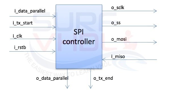
Figure 5 – SPI Controller interface
i_clk              : input clock
i_rstb             : input power on reset active low
i_tx_start         : input start sending i_data_parallel on serial line
o_tx_end           : serial data sending terminated
i_data_parallel    : parallel data to send
o_data_parallel    : parallel received data
o_sclk             : serial clock output
o_ss               : slave select
o_mosi             : serial data output
i_miso             : serial data input
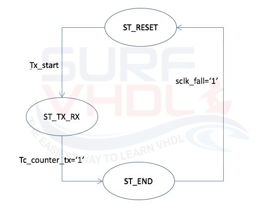
The SPI controller VHDL code will implement the FSM described in Figure 6. The input parallel data will be sent using the tx_start input signal. The FSM goes to “ST_TX_RX” state for a programmed number of clock cycles. During the data transmission, MISO input is sampled into the internal shift register. At the end of data transmission, the parallelized input is available on “o_parallel_data” output port and a pulse is generated on “o_tx_end” port.
Setting the Clock Divider (CLK_DIV)
In the VHDL code, the CLK_DIV generic plays a crucial role. It allows you to scale down your system clock (i_clk) to achieve the desired SPI Serial Clock (o_sclk) frequency. The formula to calculate it is:
o_sclk frequency = i_clk / (2 * CLK_DIV)
For example, if your FPGA runs at 50 MHz and you need an SPI clock of 1 MHz, you would set CLK_DIV = 25.
A possible VHDL implementation of the SPI controller is available below:
library ieee;
use ieee.std_logic_1164.all;
use ieee.numeric_std.all;

entity spi_controller is
generic(
  N                     : integer := 8;      -- number of bits to serialize
  CLK_DIV               : integer := 100 );  -- input clock divider to generate output serial clock; o_sclk frequency = i_clk/(2*CLK_DIV)
 port (
  i_clk                       : in  std_logic;
  i_rstb                      : in  std_logic;
  i_tx_start                  : in  std_logic;  -- start TX on serial line
  o_tx_end                    : out std_logic;  -- TX data completed; o_data_parallel available
  i_data_parallel             : in  std_logic_vector(N-1 downto 0);  -- data to send
  o_data_parallel             : out std_logic_vector(N-1 downto 0);  -- received data
  o_sclk                      : out std_logic;
  o_ss                        : out std_logic;
  o_mosi                      : out std_logic;
  i_miso                      : in  std_logic);
end spi_controller;

architecture rtl of spi_controller is

type t_spi_controller_fsm is (
                          ST_RESET   ,
                          ST_TX_RX   ,
                          ST_END     );

signal r_counter_clock        : integer range 0 to CLK_DIV*2;
signal r_sclk_rise            : std_logic;
signal r_sclk_fall            : std_logic;
signal r_counter_clock_ena    : std_logic;

signal r_counter_data         : integer range 0 to N;
signal w_tc_counter_data      : std_logic;

signal r_st_present           : t_spi_controller_fsm;
signal w_st_next              : t_spi_controller_fsm;
signal r_tx_start             : std_logic;  -- start TX on serial line
signal r_tx_data              : std_logic_vector(N-1 downto 0);  -- data to send
signal r_rx_data              : std_logic_vector(N-1 downto 0);  -- received data

begin

w_tc_counter_data  <= '0' when(r_counter_data>0) else '1';
--------------------------------------------------------------------
-- FSM
p_state : process(i_clk,i_rstb)
begin
  if(i_rstb='0') then
    r_st_present            <= ST_RESET;
  elsif(rising_edge(i_clk)) then
    r_st_present            <= w_st_next;
  end if;
end process p_state;

p_comb : process(
                 r_st_present                       ,
                 w_tc_counter_data                  ,
                 r_tx_start                         ,
                 r_sclk_rise                        ,
                 r_sclk_fall                         )
begin
  case r_st_present is
    when  ST_TX_RX      =>
      if       (w_tc_counter_data='1') and (r_sclk_rise='1') then  w_st_next  <= ST_END       ;
      else                                                         w_st_next  <= ST_TX_RX     ;
      end if;

    when  ST_END      =>
      if(r_sclk_fall='1') then
        w_st_next  <= ST_RESET    ;
      else
        w_st_next  <= ST_END    ;
      end if;

    when  others            =>  -- ST_RESET
      if(r_tx_start='1') then   w_st_next  <= ST_TX_RX ;
      else                      w_st_next  <= ST_RESET ;
      end if;
  end case;
end process p_comb;

p_state_out : process(i_clk,i_rstb)
begin
  if(i_rstb='0') then
    r_tx_start           <= '0';
    r_tx_data            <= (others=>'0');
    r_rx_data            <= (others=>'0');
    o_tx_end             <= '0';
    o_data_parallel      <= (others=>'0');

    r_counter_data       <= N-1;
    r_counter_clock_ena  <= '0';

    o_sclk               <= '1';
    o_ss                 <= '1';
    o_mosi               <= '1';
  elsif(rising_edge(i_clk)) then
    r_tx_start           <= i_tx_start;

    case r_st_present is
      when ST_TX_RX         =>
        o_tx_end             <= '0';
        r_counter_clock_ena  <= '1';
        if(r_sclk_rise='1') then
          o_sclk               <= '1';
          r_rx_data            <= r_rx_data(N-2 downto 0)&i_miso;
          if(r_counter_data>0) then
            r_counter_data       <= r_counter_data - 1;
          end if;
        elsif(r_sclk_fall='1') then
          o_sclk               <= '0';
          o_mosi               <= r_tx_data(N-1);
          r_tx_data            <= r_tx_data(N-2 downto 0)&'1';
        end if;
        o_ss                 <= '0';

      when ST_END          =>
        o_tx_end             <= r_sclk_fall;
        o_data_parallel      <= r_rx_data;
        r_counter_data       <= N-1;
        r_counter_clock_ena  <= '1';
        o_ss                 <= '0';

      when others               =>  -- ST_RESET
        r_tx_data            <= i_data_parallel;
        o_tx_end             <= '0';
        r_counter_data       <= N-1;
        r_counter_clock_ena  <= '0';

        o_sclk               <= '1';
        o_ss                 <= '1';
        o_mosi               <= '1';
    end case;
  end if;
end process p_state_out;


p_counter_clock : process(i_clk,i_rstb)
begin
  if(i_rstb='0') then
    r_counter_clock            <= 0;
    r_sclk_rise                <= '0';
    r_sclk_fall                <= '0';
  elsif(rising_edge(i_clk)) then
    if(r_counter_clock_ena='1') then  -- sclk = '1' by default
      if(r_counter_clock=CLK_DIV-1) then  -- first edge = fall
        r_counter_clock            <= r_counter_clock + 1;
        r_sclk_rise                <= '0';
        r_sclk_fall                <= '1';
      elsif(r_counter_clock=(CLK_DIV*2)-1) then
        r_counter_clock            <= 0;
        r_sclk_rise                <= '1';
        r_sclk_fall                <= '0';
      else
        r_counter_clock            <= r_counter_clock + 1;
        r_sclk_rise                <= '0';
        r_sclk_fall                <= '0';
      end if;
    else
      r_counter_clock            <= 0;
      r_sclk_rise                <= '0';
      r_sclk_fall                <= '0';
    end if;
  end if;
end process p_counter_clock;

end rtl;
To verify the correct behavior of the SPI controller before moving to hardware synthesis, a proper testbench is required.
How to Design SPI Controller in VHDL
Get the complete VHDL code from this article.
In the following figures, there are three examples of SPI protocol simulation. The Modelsim windows clearly show the SPI protocol behavior: input parallel data is serialized on the MOSI output port. The MISO input data is parallelized in the o_parallel_data port of the SPI controller.
Simulation Results
Figure 7 shows an overall simulation view of three SPI cycles.
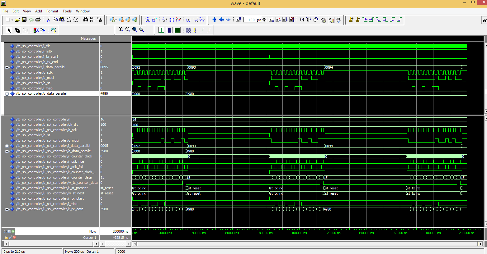
Figure 7 – SPI Controller Modelsim simulation – All view
Figure 8 shows a zoom on the second SPI cycle.
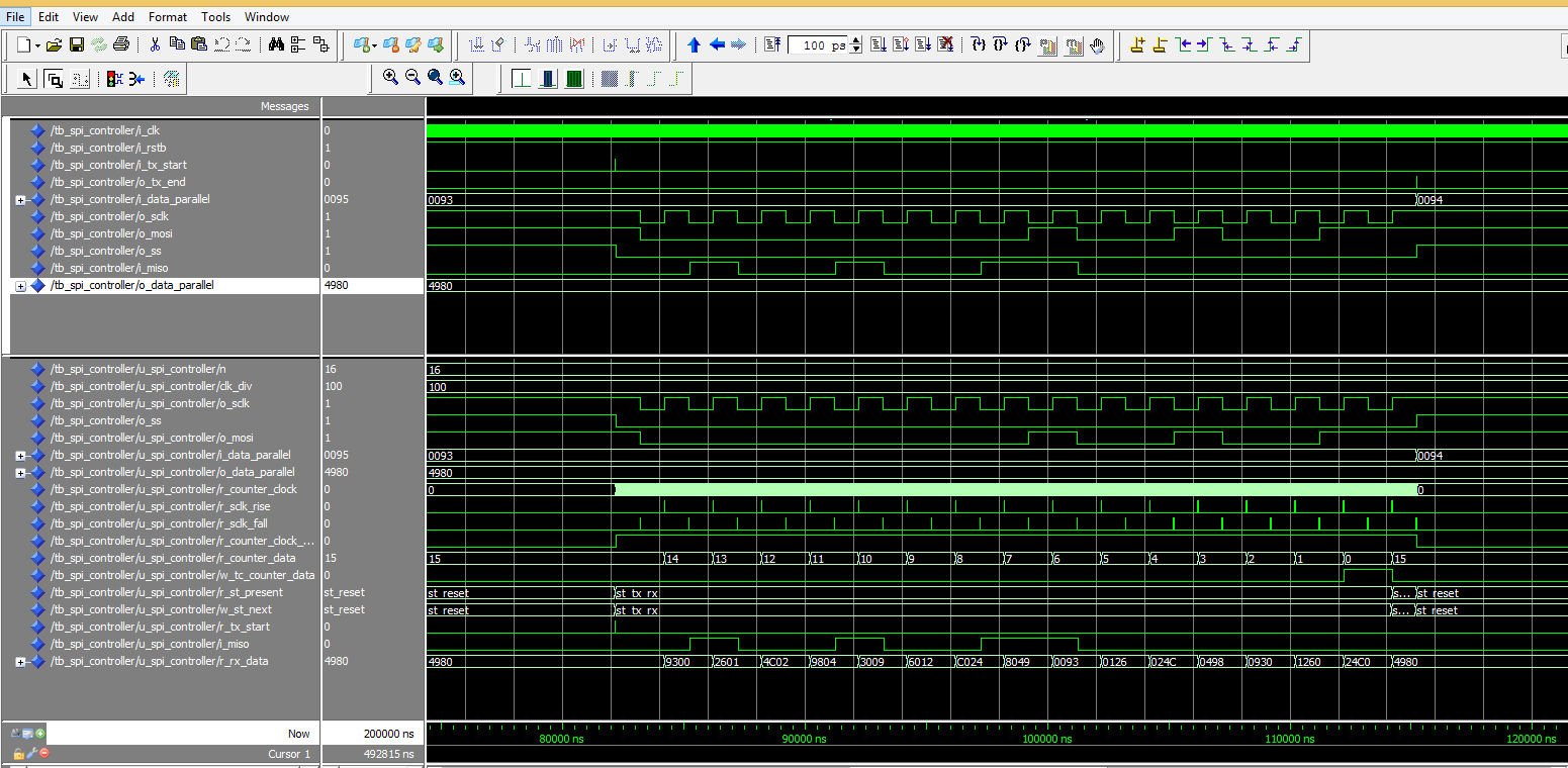
Figure – 8 SPI Controller Modelsim simulation – zoom one cycle
Figure 9 shows a zoom on the SPI cycle start. The system clock is set to 10 ns in the simulation. The SCLK is generated by dividing the system clock by 200: 100 for the high phase and 100 for the low phase, as specified in the generic “CLK_DIV”.
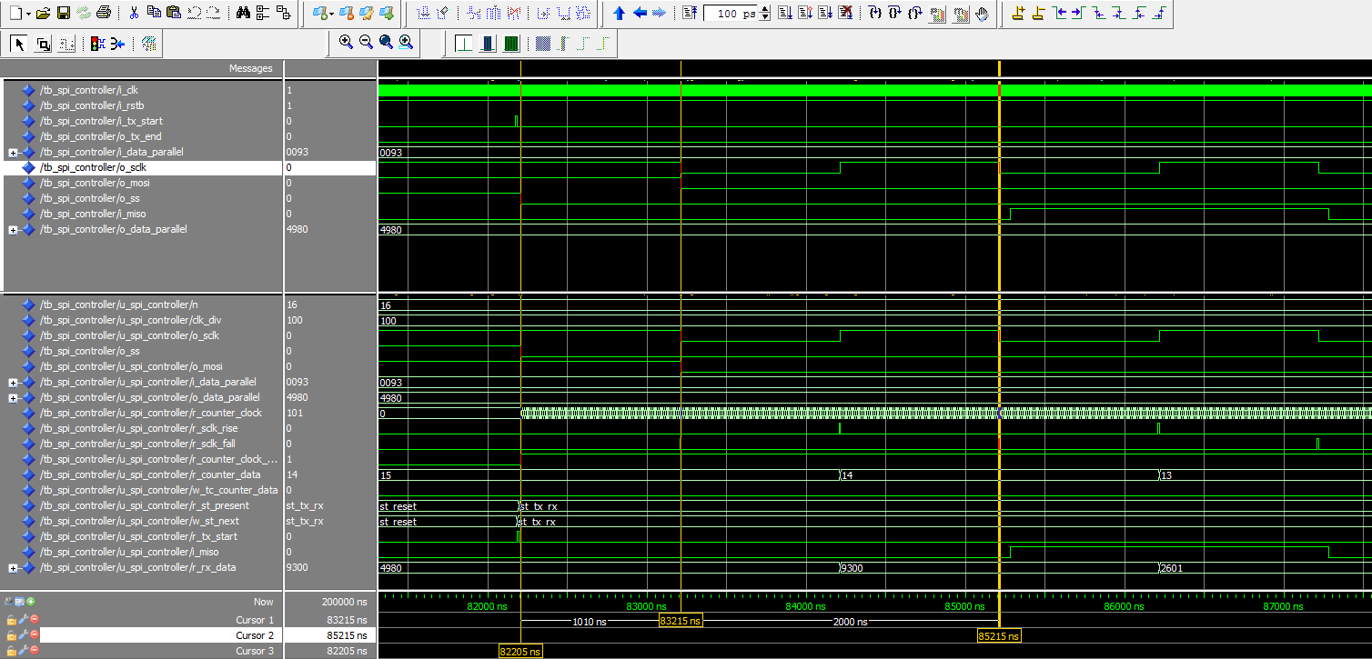
Figure 9 – SPI Controller Modelsim simulation – cycle start
The SPI controller VHDL code above is technology-independent and can be implemented either on FPGA or ASIC.
Figure 10 shows the Altera Quartus II RTL viewer of the SPI VHDL code implementation above.
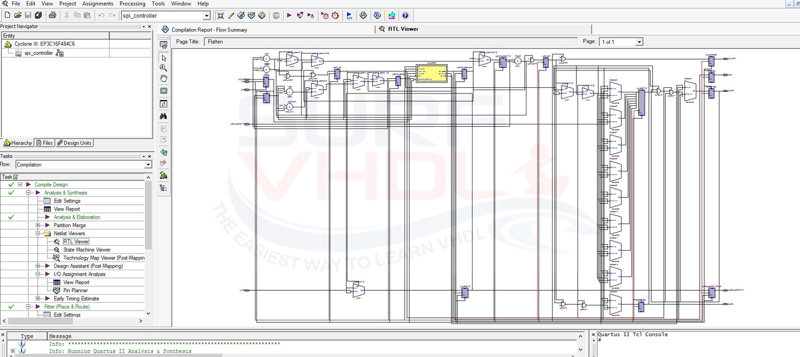
Figure 10 – SPI Controller Quartus II RTL viewer
The SPI controller VHDL code has been tested on Altera Cyclone III FPGA with 8-bit serial and parallel data.
The implementation takes 58 Logic Elements (LEs) and operates at 400 MHz as reported in the Quartus II area report and timing report below.
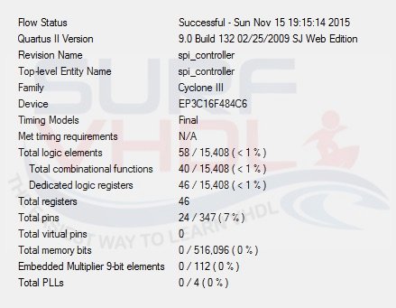
Figure – 11 SPI Controller Altera Quartus II -Area report for Cyclone III

Figure – 12 SPI Controller Altera Quartus II -Timing report for Cyclone III
References:
https://en.wikipedia.org/wiki/Serial_Peripheral_Interface_Bus
If you appreciate this post, please help me share it with your friends.
If you need to contact me, please write to: surf.vhdl@gmail.com