
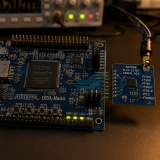
Connection of Serial ADC to FPGA
An ADC (Analog to Digital Converter) can be interfaced to an FPGA or ASIC in different ways depending on the output interface. This post gives an overview of the different interfaces available in ADC interfacing.
In modern ADCs, when the sampling rate is below 10 Msample/sec, the devices often implement a serial interface to provide sampled data to the user. The serial interface is slightly more complex than a parallel interface but using a serial protocol reduces the number of wires and allows interfacing the ADC to a microprocessor like Arduino or Raspberry Pi.
In the serial interface setup, the serial clock provided by the host device connected to the ADC is also used as the ADC sampling clock.
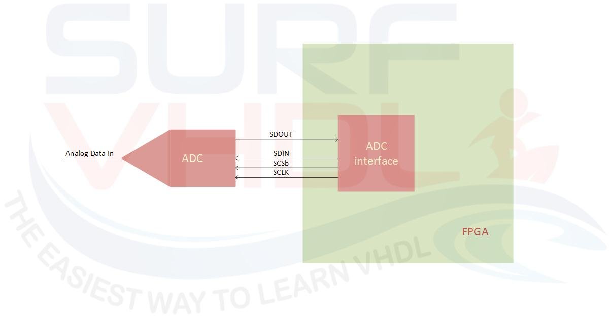
Figure1 – Serial ADC connected to FPGA
In this post, we will see an example of how to interface the TI ADC128S022 used on the Altera DE0-nano Board.
TI ADC128S022 Features and Architecture
The ADC128S022 device is a low-power, eight-channel CMOS 12-bit analog-to-digital converter specified for conversion throughput rates of 50 ksps to 200 ksps. The converter is based on a successive approximation register (SAR) architecture with an internal track-and-hold circuit. It can be configured to accept up to eight input signals at inputs IN0 through IN7.
The output serial data is straight binary and is compatible with several standards, such as SPI, QSPI, MICROWIRE, and many common DSP serial interfaces.
ADC Serial Protocol
The ADC serial protocol is a simple SPI protocol.
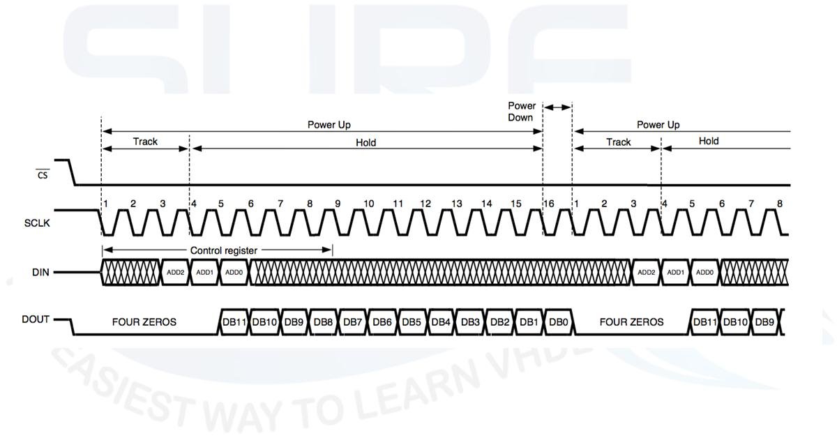
Figure2 – ADC128S022 Serial Protocol
During the first 3 cycles of SCLK, the ADC is in track mode, acquiring the input voltage. For the next 13 SCLK cycles the conversion is accomplished and the data is clocked out. The SCLK falling edges 1 through 4 clock out leading zeros while falling edges 5 through 16 clock out the conversion result, MSB first. If there is more than one conversion in a frame (continuous conversion mode as in the figure), the ADC will re-enter the track mode on the falling edge of SCLK after the N*16th rising edge of SCLK and re-enter the hold/convert mode on the N*16+4th falling edge of SCLK. “N” is an integer value. You can find more information on the SPI ADC128S022 protocol in the datasheet.
Interactive ADC128S022 SPI Sequence
ADC128S022 controller VHDL implementation
In order to convert and read the sampled data from the ADC, the protocol of Figure2 shall be implemented. On DE0-nano, the board clock is 50 MHz.
The ADC128S022 can work from 0.8 MHz to 3.2 MHz. Using the board clock we can generate the maximum sampling clock as 50/16 = 3.125 MHz.
In this example, the VHDL code of the serial ADC controller is implemented using 5 main blocks, each implemented as a VHDL process:
- p_conversion_control (Control Logic): Clock generation is enabled using an input control signal
i_conv_ena. When the conversion is disabled, the control logic will complete the current conversion before stopping the process. - p_counter_data: Counts the current clock rising edge and controls the data conversion. The counter is used as a sequencer for the current conversion state.
- p_serial_input: The input ADC channel is sampled before starting the conversion and provided to the ADC via the serial output data line. The
r_counter_datainternal counter demuxes the input serial data into a parallel register. At the end of the conversion, the receivedr_adc_datais stored in the output parallel 12-bit registero_adc_data. - p_serial_output: Drives the serial clock output and serial data output to the ADC.
- p_counter_clock (Serial Clock Generator): The serial clock is generated by dividing the board clock. The clock generation is disabled if no conversion is required.
library ieee;
use ieee.std_logic_1164.all;
use ieee.numeric_std.all;

entity adc_serial_control is
generic(
  CLK_DIV               : integer := 100 );  -- input clock divider to generate output serial clock; o_sclk frequency = i_clk/(CLK_DIV)
port (
  i_clk                       : in  std_logic;
  i_rstb                      : in  std_logic;
  i_conv_ena                  : in  std_logic;  -- enable ADC convesion
  i_adc_ch                    : in  std_logic_vector(2 downto 0);  -- ADC channel 0-7
  o_adc_data_valid            : out std_logic;  -- conversion valid pulse
  o_adc_ch                    : out std_logic_vector(2 downto 0);  -- ADC converted channel
  o_adc_data                  : out std_logic_vector(11 downto 0); -- adc parallel data
-- ADC serial interface
  o_sclk                      : out std_logic;
  o_ss                        : out std_logic;
  o_mosi                      : out std_logic;
  i_miso                      : in  std_logic);
end adc_serial_control;

architecture rtl of adc_serial_control is
constant C_N                     : integer := 16;

signal r_counter_clock            : integer range 0 to CLK_DIV;
signal r_sclk_rise                : std_logic;
signal r_sclk_fall                : std_logic;
signal r_counter_clock_ena        : std_logic;

signal r_counter_data             : integer range 0 to C_N-1;
signal r_tc_counter_data          : std_logic;

signal r_conversion_running       : std_logic;  -- enable serial data protocol

signal r_miso                     : std_logic;
signal r_conv_ena                 : std_logic;  -- enable ADC convesion
signal r_adc_ch                   : std_logic_vector(2 downto 0);  -- ADC converted channel
signal r_adc_data                 : std_logic_vector(11 downto 0); -- adc parallel data

begin

--------------------------------------------------------------------
-- FSM
p_conversion_control : process(i_clk,i_rstb)
begin
  if(i_rstb='0') then
    r_conv_ena             <= '0';
    r_conversion_running   <= '0';
    r_counter_clock_ena    <= '0';
  elsif(rising_edge(i_clk)) then
    r_conv_ena             <= i_conv_ena;
    if(r_conv_ena='1') then
      r_conversion_running   <= '1';
    elsif(r_conv_ena='0') and (r_tc_counter_data='1') then -- terminate current conversion
      r_conversion_running   <= '0';
    end if;

    r_counter_clock_ena    <= r_conversion_running;  -- enable clock divider

  end if;
end process p_conversion_control;

p_counter_data : process(i_clk,i_rstb)
begin
  if(i_rstb='0') then
    r_counter_data       <= 0;
    r_tc_counter_data    <= '0';
  elsif(rising_edge(i_clk)) then
    if(r_counter_clock_ena='1') then
      if(r_sclk_rise='1') then  -- count data @ o_sclk rising edge
        if(r_counter_data<C_N-1) then
          r_counter_data     <= r_counter_data + 1;
          r_tc_counter_data  <= '0';
        else
          r_counter_data     <= 0;
          r_tc_counter_data  <= '1';
        end if;
      else
        r_tc_counter_data  <= '0';
      end if;
    else
      r_counter_data     <= 0;
      r_tc_counter_data  <= '0';
    end if;
  end if;
end process p_counter_data;

-- Serial Input Process
p_serial_input : process(i_clk,i_rstb)
begin
  if(i_rstb='0') then
    r_miso               <= '0';
    r_adc_ch             <= (others=>'0');
    r_adc_data           <= (others=>'0');
  elsif(rising_edge(i_clk)) then
    r_miso               <= i_miso;

    if(r_tc_counter_data='1') then
      r_adc_ch             <= i_adc_ch; -- strobe new
    end if;

    case r_counter_data is
      when  4  => r_adc_data(11)  <= r_miso;
      when  5  => r_adc_data(10)  <= r_miso;
      when  6  => r_adc_data( 9)  <= r_miso;
      when  7  => r_adc_data( 8)  <= r_miso;
      when  8  => r_adc_data( 7)  <= r_miso;
      when  9  => r_adc_data( 6)  <= r_miso;
      when 10  => r_adc_data( 5)  <= r_miso;
      when 11  => r_adc_data( 4)  <= r_miso;
      when 12  => r_adc_data( 3)  <= r_miso;
      when 13  => r_adc_data( 2)  <= r_miso;
      when 14  => r_adc_data( 1)  <= r_miso;
      when 15  => r_adc_data( 0)  <= r_miso;
      when others => NULL;
    end case;
  end if;
end process p_serial_input;

-- SERIAL Output process
p_serial_output : process(i_clk,i_rstb)
begin
  if(i_rstb='0') then
    o_ss                 <= '1';
    o_mosi               <= '1';
    o_sclk               <= '1';
    o_adc_data_valid     <= '0';
    o_adc_ch             <= (others=>'0');
    o_adc_data           <= (others=>'0');
  elsif(rising_edge(i_clk)) then
    o_ss                 <= not r_conversion_running;

    if(r_tc_counter_data='1') then
      o_adc_ch             <= r_adc_ch; -- update current conversion
      o_adc_data           <= r_adc_data;
    end if;
    o_adc_data_valid     <= r_tc_counter_data;

    if(r_counter_clock_ena='1') then  -- sclk = '1' by default
      if(r_sclk_rise='1') then
        o_sclk   <= '1';
      elsif(r_sclk_fall='1') then
        o_sclk   <= '0';
      end if;
    else
      o_sclk   <= '1';
    end if;

    if(r_sclk_fall='1') then
      case r_counter_data is
        when  2  => o_mosi <= r_adc_ch(2);
        when  3  => o_mosi <= r_adc_ch(1);
        when  4  => o_mosi <= r_adc_ch(0);
        when others => NULL;
      end case;
    end if;
  end if;
end process p_serial_output;

-- CLOCK divider
p_counter_clock : process(i_clk,i_rstb)
begin
  if(i_rstb='0') then
    r_counter_clock            <= 0;
    r_sclk_rise                <= '0';
    r_sclk_fall                <= '0';
  elsif(rising_edge(i_clk)) then
    if(r_counter_clock_ena='1') then
      if(r_counter_clock=(CLK_DIV/2)-1) then  -- firse edge = fall
        r_counter_clock            <= r_counter_clock + 1;
        r_sclk_rise                <= '0';
        r_sclk_fall                <= '1';
      elsif(r_counter_clock=(CLK_DIV-1)) then
        r_counter_clock            <= 0;
        r_sclk_rise                <= '1';
        r_sclk_fall                <= '0';
      else
        r_counter_clock            <= r_counter_clock + 1;
        r_sclk_rise                <= '0';
        r_sclk_fall                <= '0';
      end if;
    else
      r_counter_clock            <= 0;
      r_sclk_rise                <= '0';
      r_sclk_fall                <= '0';
    end if;
  end if;
end process p_counter_clock;

end rtl;
How to Connect a Serial ADC to an FPGA
Get the complete VHDL code from this article.
Serial ADC controller VHDL code Simulation
In the simulation window, the board clock is 50 MHz (20 ns). The clock division factor is 16 so the generated serial clock will be 3.125 MHz (i.e. 320 ns)
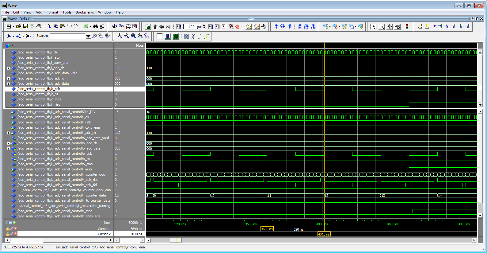
Figure3 – Serial ADC controller Simulation
Serial ADC controller VHDL code implementation on FPGA
The DE0-nano provides 8 LEDs. In order to verify the ADC controller VHDL code, the 8 LEDs of the board are connected to the 8 ADC MSB, so we can use the LEDs to “read” the ADC converted values.
The ADC channel is selected using the switch SW 3..1 that will select the serial ADC input channel 0 to 7. The Serial ADC conversion is controlled using SW4 that can enable/disable the ADC conversion.
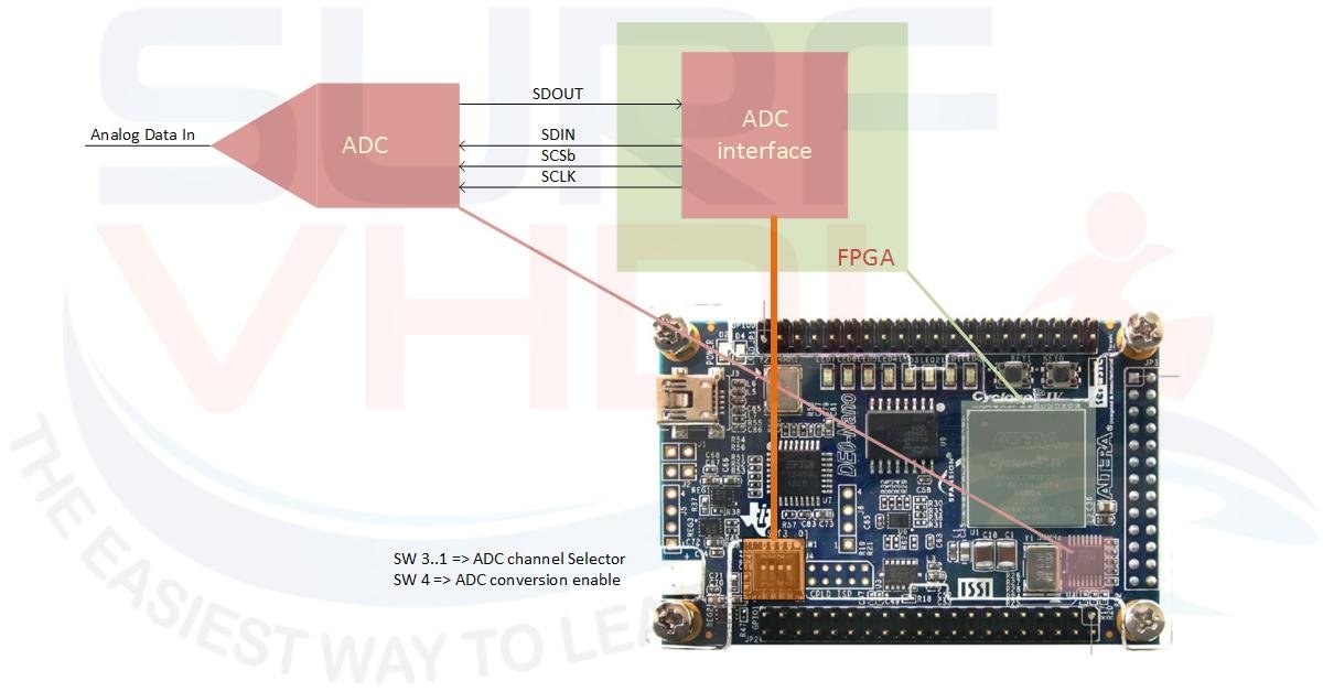
Figure4 – DE0 nano Serial ADC implementation architecture
Conclusion
Interfacing a serial ADC to an FPGA requires a solid understanding of the SPI protocol and precise timing management. In this post, we explored the TI ADC128S022 architecture, analyzed its serial tracking and conversion cycles, and implemented a robust, modular VHDL controller.
By structuring the VHDL code into 5 dedicated processes — handling control logic, data counting, serial input/output, and clock generation — the design remains clean and easy to adapt for other SPI-based ADCs. Finally, verifying the logic through a testbench simulation ensures that the physical implementation on boards like the Altera DE0-Nano behaves exactly as expected.
Video Tutorial
Watch the video below to see the serial ADC VHDL controller in action on the DE0-nano board: