Debugging an FIR in FPGA
The VHDL, and other hardware description languages such as Verilog, SistemVerolog and so on, allow us to simulate your digital design in a very accurate way.
If you write a good VHDL code after the simulation you are very confident that your VHDL design will work as it should. When you go to silicon often there are problems and you should debug your VHDL code.
Here you can find some of the common issues you have during the test of VHDL design on FPGA. The modern FPGAs allow the user to enable debug facility inside the silicon using a proprietary debug tool very like an embedded logic state analyzer.
Using Altera Quartus II you can enable the Signal Tap Analyzer or the equivalent using Xilinx Chipscope.

In this post, we are going to see an example of how to debug an FIR using the push button and the seven-segment display of a typical demo board with an FPGA, implementing a complete VHDL test bench that will be implemented in a Terasic DE0 board.
Of course, this is a didactic example, in normal work we do not verify the behaviour of a filter using a seven-segment display, but it could be a good exercise you can do to improve your skill and understand better the FIR filter and VHDL behaviour.
Before starting, you can read this post, where you can find the implementation of a template of a FIR in VHDL.
Filter Test Bench
If we want to test the FIR filter, we need to provide the input stimuli and store the output in a buffer. The data stored in the output buffer will be read out and output using the seven segments. The example will be implemented using the Terasic DE0 board. The board provides four seven-segment displays, 10 switches, and 3 push buttons.
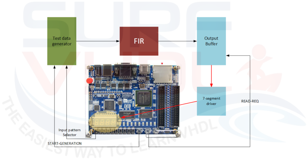
In Figure 1 the green box implements the input data generator to the FIR. In this example, we are going to implement two different inputs:
- Delta
- Step
These two stimuli are selected using the input switch. After selecting the switch, and pushing the button the selected input will be played into the FIR and acquired by the output buffer as in Figure 2. The data stored in the output buffer can be displayed in the seven-segment display at each press of the push button.
For output buffer implementation, we use both a FIFO or a dual port memory plus a simple control logic.
Since the memory is much more portable than VHDL code implementation, we are going to implement this solution as in Figure 3.
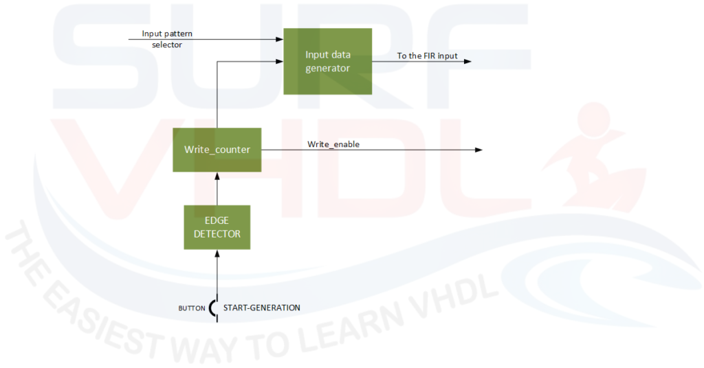
The push button input needs to be connected to an edge detector to generate a pulse in the system clock domain.
If you need to understand better this basic concept you can watch the free course
How to implement your first VHDL design
If you appreciate this post, please help us to share it with your friend.
FIR Input data generator VHDL implementation
The input test data will be generated using a component able to play the two different inputs to the filter
- Delta
- Step
The data is generated using a counter that addresses the LUT (Look-Up-Table) selected by the “i_pattern_sel” input switch:
“C_PATTERN_DELTA” and “C_PATTERN_STEP”.
As you can understand, you can implement different input patterns by adding or modifying the content of the LUT.
The architecture is very simple and can be implemented in VHDL as the code below.
library ieee;
use ieee.std_logic_1164.all;
use ieee.numeric_std.all;

entity fir_test_data_generator is
port (
  i_clk                   : in  std_logic;
  i_rstb                  : in  std_logic;
  i_pattern_sel           : in  std_logic;  -- '0'=> delta; '1'=> step
  i_start_generation      : in  std_logic;
  o_data                  : out std_logic_vector( 7 downto 0); -- to FIR
  o_write_enable          : out std_logic);  -- to the output buffer
end fir_test_data_generator;

architecture rtl of fir_test_data_generator is

type t_pattern_input is array(0 to 31) of integer range -128 to 127;

constant C_PATTERN_DELTA     : t_pattern_input := (
     0  ,
   127  ,
     0  ,
     0  ,
     0  ,
     0  ,
     0  ,
     0  ,
     0  ,
     0  ,
     0  ,
     0  ,
     0  ,
     0  ,
     0  ,
     0  ,
     0  ,
     0  ,
     0  ,
     0  ,
     0  ,
     0  ,
     0  ,
     0  ,
     0  ,
     0  ,
     0  ,
     0  ,
     0  ,
     0  ,
     0  ,
     0  );

constant C_PATTERN_STEP      : t_pattern_input := (
     0  ,
   127  ,
   127  ,
   127  ,
   127  ,
   127  ,
   127  ,
   127  ,
   127  ,
   127  ,
   127  ,
   127  ,
   127  ,
   127  ,
   127  ,
   127  ,
   127  ,
     0  ,
     0  ,
     0  ,
     0  ,
     0  ,
     0  ,
     0  ,
     0  ,
     0  ,
     0  ,
     0  ,
     0  ,
     0  ,
     0  ,
     0  );

component edge_detector
port (
  i_clk                       : in  std_logic;
  i_rstb                      : in  std_logic;
  i_input                     : in  std_logic;
  o_pulse                     : out std_logic);
end component;

signal r_write_counter             : integer range 0 to 31;
signal r_write_counter_ena         : std_logic;
signal w_start_pulse               : std_logic;

begin

u_edge_detector : edge_detector
port map(
  i_clk                       => i_clk                       ,
  i_rstb                      => i_rstb                      ,
  i_input                     => i_start_generation          ,
  o_pulse                     => w_start_pulse               );

p_write_counter : process (i_rstb,i_clk)
begin
  if(i_rstb='0') then
    r_write_counter             <= 31;
    r_write_counter_ena         <= '0';
  elsif(rising_edge(i_clk)) then
    if(w_start_pulse='1') then
      r_write_counter             <= 0;
      r_write_counter_ena         <= '1';
    elsif(r_write_counter<31) then
      r_write_counter             <= r_write_counter + 1;
      r_write_counter_ena         <= '1';
    else
      r_write_counter_ena         <= '0';
    end if;
  end if;
end process p_write_counter;

p_output : process (i_rstb,i_clk)
begin
  if(i_rstb='0') then
    o_data          <= (others=>'0');
    o_write_enable  <= '0';
  elsif(rising_edge(i_clk)) then
    o_write_enable  <= r_write_counter_ena;
    if(i_pattern_sel='0') then
      o_data     <= std_logic_vector(to_signed(C_PATTERN_DELTA(r_write_counter),8));
    else
      o_data     <= std_logic_vector(to_signed(C_PATTERN_STEP(r_write_counter),8));
    end if;
  end if;
end process p_output;

end rtl;
The “i_start_generation” signal is connected to the edge_detector in order to detect the push action on the push button.
You can find a complete VHDL description of the edge detector in this post, where you can download the VHDL code.
The output signal “o_write_enable” is used as enable signal of the output buffer. The signal is connected to the write address counter of the output buffer as will be clear next.
The “r_write_counter” accumulator is used to point the LUT. The counter values start from zero and stop when the counter reaches the value 31 which is the last address value of the LUT.
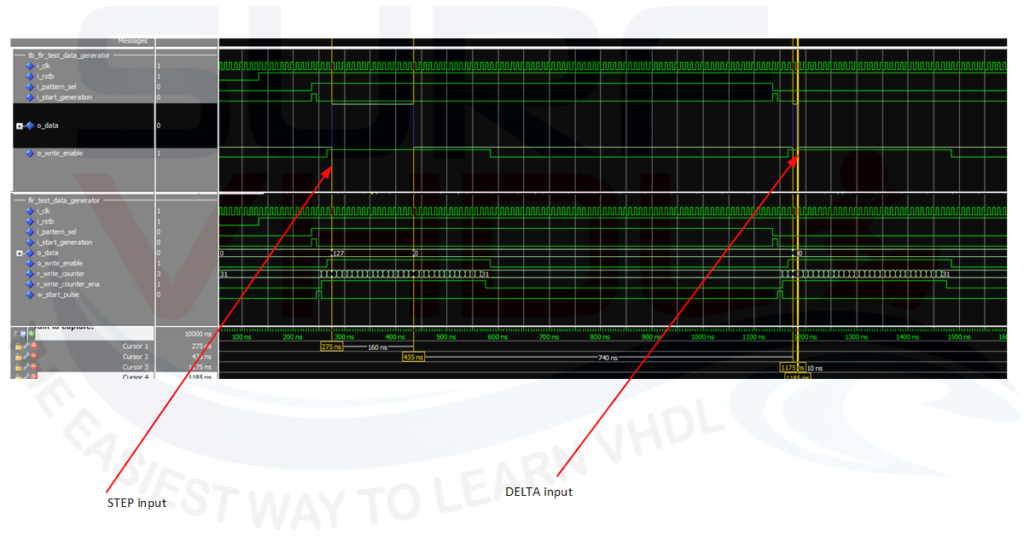
In Figure 4 is reported the simulation using when the STEP input is selected and then when the DELTA input is selected.
As clear the STEP input provides an output value of +127 for 16 clock cycles, while the DELTA input provides an output value of +127 for only one clock cycle.
The clock period is 10 ns.
If you appreciate this post, please help us to share it with your friend.
FIR test bench output buffer VHDL implementation
The output buffer is used to store the Filter output response. The system shall be able to store the filter output that is generated as “continuous play”.
The “o_write_enable” signal generated from the input data generator is used to control the write counter address generator and to enable the writing to the output buffer.
Since the data need to be displayed on the seven-segment display, we need to implement a system to read back the output buffer using an external control, in this case, the external push button.
Even in this case, we need an edge detector to read from the memory each time we push the external button.
The edge detector will increment a read counter that addresses the output buffer memory.
The read value is used to drive the 7-segment driver of Figure 1.
The output buffer memory is implemented in 32 memory locations.
library ieee;
use ieee.std_logic_1164.all;
use ieee.numeric_std.all;

entity fir_output_buffer is
port (
  i_clk                   : in  std_logic;
  i_rstb                  : in  std_logic;
  i_write_enable          : in  std_logic;
  i_data                  : in  std_logic_vector( 9 downto 0); -- from FIR
  i_read_request          : in  std_logic;
  o_data                  : out std_logic_vector( 9 downto 0); -- to seven segment
  o_test_add              : out std_logic_vector( 4 downto 0)); -- test read address
end fir_output_buffer;

architecture rtl of fir_output_buffer is

type t_output_buffer_mem is array(0 to 31) of std_logic_vector( 9 downto 0);


component edge_detector
port (
  i_clk                       : in  std_logic;
  i_rstb                      : in  std_logic;
  i_input                     : in  std_logic;
  o_pulse                     : out std_logic);
end component;

signal output_buffer_mem           : t_output_buffer_mem ;

signal r_write_add                 : integer range 0 to 31;

signal r_read_add                  : integer range 0 to 31;
signal w_read_pulse                : std_logic;

begin

u_edge_detector : edge_detector
port map(
  i_clk                       => i_clk                       ,
  i_rstb                      => i_rstb                      ,
  i_input                     => i_read_request              ,
  o_pulse                     => w_read_pulse                );

p_write_counter : process (i_rstb,i_clk)
begin
  if(i_rstb='0') then
    r_write_add             <= 0;
  elsif(rising_edge(i_clk)) then
    if(i_write_enable='1') then
      if(r_write_add<31) then
        r_write_add             <= r_write_add + 1;
      end if;
    else
      r_write_add             <= 0;
    end if;
  end if;
end process p_write_counter;

p_read_counter : process (i_rstb,i_clk)
begin
  if(i_rstb='0') then
    r_read_add             <= 0;
  elsif(rising_edge(i_clk)) then
    if(w_read_pulse='1') then
      if(r_read_add<31) then
        r_read_add             <= r_read_add + 1;
      else
        r_read_add             <= 0;
      end if;
    end if;
  end if;
end process p_read_counter;

p_memory : process (i_clk)
begin
  if(rising_edge(i_clk)) then
    if(i_write_enable='1') then
      output_buffer_mem(r_write_add)  <= i_data;
    end if;

    o_data  <= output_buffer_mem(r_read_add);
    end if;
end process p_memory;

o_test_add  <= std_logic_vector(to_unsigned(r_read_add,5));

end rtl;
In the VHDL implementation the read counter wrap-around when reaches the value 31, so by pushing the external button we can read back the output buffer continuously. In order to understand what is the value read from the output buffer, we are connecting also the memory address to the seven-segment display
Figure 5 reports the stand-alone simulation of the output buffer. In the top view of the figure is reported the input. Only 32 values of input data are stored in the buffer. As clear the write address counter stops when the counter value reaches the value 31. Pay attention that address 31 is overwritten until the “i_write_enable” input control signal is high. The bottom of the figure reports the read-out phase of the output buffer. As clear address 31 of the output buffer contains the value “54” i.e. the last value in input with the “i_write_enable” control signal high.
FIR test bench complete VHDL implementation
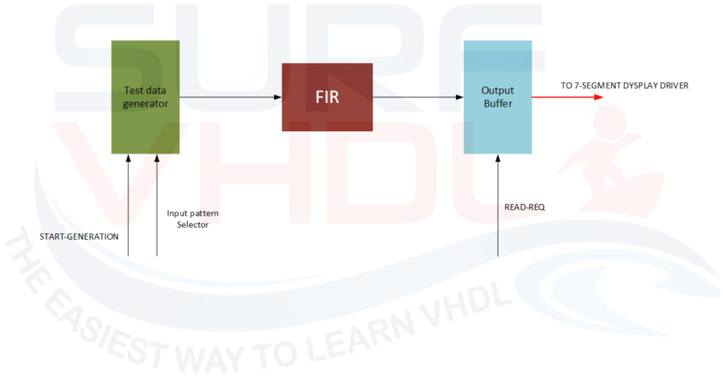
In this section, we are going to integrate the previous section with the FIR filter implemented in this post, realizing the complete test bench that can be instantiated inside the FPGA top-level implementation. Figure 6 shows the architecture of the FIR test bench we are going to implement.
This block can be instantiated as in Figure 1 in the FPGA top level. You can download a fully functional example on Terasic DE0 board in the box below.
library ieee;
use ieee.std_logic_1164.all;
use ieee.numeric_std.all;

entity fir_filter_test is
port (
  i_clk                   : in  std_logic;
  i_rstb                  : in  std_logic;
  i_pattern_sel           : in  std_logic;  -- '0'=> delta; '1'=> step
  i_start_generation      : in  std_logic;
  i_read_request          : in  std_logic;
  o_data_buffer           : out std_logic_vector( 9 downto 0); -- to seven segment
  o_test_add              : out std_logic_vector( 4 downto 0)); -- test read address
end fir_filter_test;

architecture rtl of fir_filter_test is

constant C_COEFF_0    : std_logic_vector( 7 downto 0):= std_logic_vector(to_signed(-10,8));
constant C_COEFF_1    : std_logic_vector( 7 downto 0):= std_logic_vector(to_signed(110,8));
constant C_COEFF_2    : std_logic_vector( 7 downto 0):= std_logic_vector(to_signed(127,8));
constant C_COEFF_3    : std_logic_vector( 7 downto 0):= std_logic_vector(to_signed(-20,8));

component fir_test_data_generator
port (
  i_clk                   : in  std_logic;
  i_rstb                  : in  std_logic;
  i_pattern_sel           : in  std_logic;  -- '0'=> delta; '1'=> step
  i_start_generation      : in  std_logic;
  o_data                  : out std_logic_vector( 7 downto 0); -- to FIR
  o_write_enable          : out std_logic);  -- to the output buffer
end component;

component fir_filter_4
port (
  i_clk        : in  std_logic;
  i_rstb       : in  std_logic;
  -- coefficient
  i_coeff_0    : in  std_logic_vector( 7 downto 0);
  i_coeff_1    : in  std_logic_vector( 7 downto 0);
  i_coeff_2    : in  std_logic_vector( 7 downto 0);
  i_coeff_3    : in  std_logic_vector( 7 downto 0);
  -- data input
  i_data       : in  std_logic_vector( 7 downto 0);
  -- filtered data
  o_data       : out std_logic_vector( 9 downto 0));
end component;

component fir_output_buffer
port (
  i_clk                   : in  std_logic;
  i_rstb                  : in  std_logic;
  i_write_enable          : in  std_logic;
  i_data                  : in  std_logic_vector( 9 downto 0); -- from FIR
  i_read_request          : in  std_logic;
  o_data                  : out std_logic_vector( 9 downto 0); -- to seven segment
  o_test_add              : out std_logic_vector( 4 downto 0)); -- test read address
end component;

signal w_write_enable          : std_logic;
signal w_data_test             : std_logic_vector( 7 downto 0);
signal w_data_filter           : std_logic_vector( 9 downto 0);

begin

u_fir_test_data_generator : fir_test_data_generator
port map(
  i_clk                   => i_clk                   ,
  i_rstb                  => i_rstb                  ,
  i_pattern_sel           => i_pattern_sel           ,
  i_start_generation      => i_start_generation      ,
  o_data                  => w_data_test             ,
  o_write_enable          => w_write_enable          );

u_fir_filter_4 : fir_filter_4
port map(
  i_clk        => i_clk        ,
  i_rstb       => i_rstb       ,
  -- coefficient
  i_coeff_0    => C_COEFF_0    ,
  i_coeff_1    => C_COEFF_1    ,
  i_coeff_2    => C_COEFF_2    ,
  i_coeff_3    => C_COEFF_3    ,
  -- data input
  i_data       => w_data_test  ,
  -- filtered data
  o_data       => w_data_filter);

u_fir_output_buffer : fir_output_buffer
port map(
  i_clk                   => i_clk                   ,
  i_rstb                  => i_rstb                  ,
  i_write_enable          => w_write_enable          ,
  i_data                  => w_data_filter           ,
  i_read_request          => i_read_request          ,
  o_data                  => o_data_buffer           ,
  o_test_add              => o_test_add              );

end rtl;
The VHDL code of the filter test bench implements straight forward the architecture of Figure 6. In the VHDL we set the FIR coefficient as a constant value.
From the simulation, in Figure 7 the DELTA response of the FIR filter in the bottom view reports the filter coefficient divided by 2.
This result is clear from the filter implementation in this post.
In Figure 8 is reported the simulation with STEP input
The video shows a live demo of the VHDL implementation of the FIR filter test bench on Terasic DE0 board
Conclusion
In this post, we implemented an FIR test bench on FPGA where you can understand how to implement an FIR in VHDL and how to test the design using the capability of the demo board Terasic DE0
References
How to Implement FIR Filter in VHDL
If you appreciate this post, please help us to share it with your friend.
If you need to contact us, please write to: surf.vhdl@gmail.com
We appreciate any of your comments, please post below:


I could not find any email address in your website to contact you. SO I write it here. please delete it from here after you read it.
Main question: How can I contact you? email address???
just send an email to surf.vhdl@gmail.com
Hello Franceso,
am I right to assume, that your provided download for testing is not by itself working on a real device? the fir_filter_test.vhd does not include 7segment displays, as i see it. I was trying to make it run on my altera board, but i guess i will have to build a scheme including the test aswell as the displays. Thanks anyways for the great explanations here!
did you get the VHDL by mail?