Before reading the post, if you need the VHDL code example of the FOR-LOOP, just put your email in the box you find in the post. There is no need to post a comment asking me for the code 🙂
If you don’t receive the email, please check your SPAM folder, enjoy!
VHDL Iterative Statement
In VHDL the FOR-LOOP statement is a sequential statement that can be used inside a process statement as well as in subprograms.
The FOR-LOOP statement is used whenever an operation needs to be repeated.
In VHDL behavioral code, i.e. when we write a VHDL code of a test bench in a pure behavioral model, the FOR-LOOP usage statement can be considered as a common SW implementation of a loop statement as in the other SW languages.
In VHDL RTL the FOR-LOOP statement shall be used taking into account the final hardware implementation.

This consideration, of course, is always valid in any VHDL code implementation.
The FOR-LOOP statement is more difficult to visualize as a final result in HW implementation.
In the next section, we will learn how the FOR-LOOP statement is mapped into hardware logic using a couple of examples.
The FOR-LOOP VHDL BNF syntax is:
loop_statement ::= [ loop_label : ]
  for loop_parameter_specification loop sequence_of_statements

  end loop [ loop_label ] ;


for item in 1 to last_item loop
  table(item) := 0;
end loop;
The loop label is optional but is a good practice to use since the VHDL code became more readable even if the VHDL source file became larger (nowadays the space on the disk is cheaper than some years ago, so it is not an issue).
FOR-LOOP VHDL example
A typical example of FOR-LOOP statement is a parity checker.
A simple implementation of a parity checker on an 8-bit register can be implemented using an 8 input XOR gate as in Figure 1.
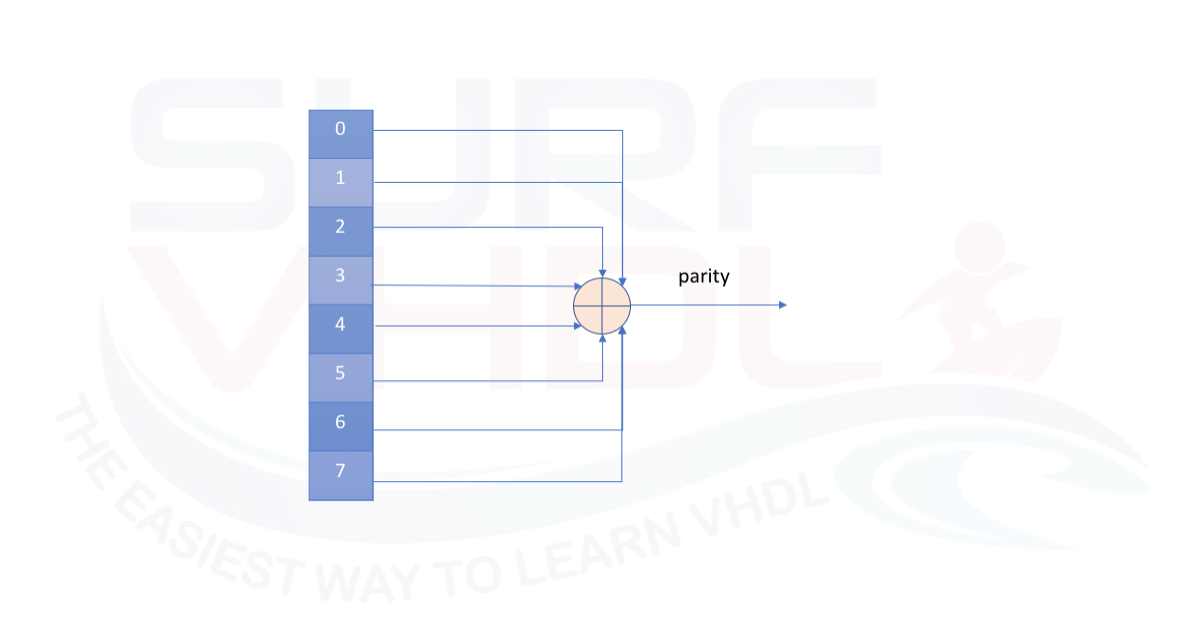
The only problem is that no all technologies offer an 8-input XOR gate.
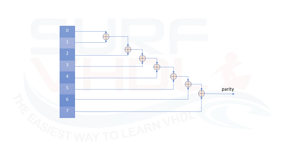
A simple possible solution could be to cascade 7 XOR port where the output of the k-th port is the input of the (k+1) XOR port as in Figure 2
library IEEE;
use IEEE.std_logic_1164.all;
use IEEE.numeric_std.all;

entity parity_check is
port(
  i_clk             : in  std_logic;
  i_data            : in  std_logic_vector(7 downto 0);
  o_parity          : out std_logic);
end parity_check;

architecture rtl of parity_check is

signal r_data            : std_logic_vector(7 downto 0);

begin

p_parity_check : process (i_clk)
variable vparity           : std_logic;
begin
  if rising_edge(i_clk) then
    r_data  <= i_data;

    vparity := '0';
    l_parity : for k in 0 to r_data'length-1 loop
      vparity := vparity xor r_data(k);
    end loop l_parity;

    o_parity <= vparity;
  end if;
end process p_parity_check;

end rtl;
VHDL code for 8-bit parity checker using FOR-LOOP
Another example is represented by a VHDL code that implements an accumulator.
The architecture is very similar to a parity checker (that can be seen as an accumulator over GF(2), i.e Galois Field of order 2) the 8-bit values are added together using the temporary variable for accumulation and then assigned to the entity output.
A possible VHDL code is reported below:
library IEEE;
use IEEE.std_logic_1164.all;
use IEEE.numeric_std.all;

entity accumulator is
port(
  i_clk             : in  std_logic;
  i_data0           : in  std_logic_vector(7 downto 0);
  i_data1           : in  std_logic_vector(7 downto 0);
  i_data2           : in  std_logic_vector(7 downto 0);
  i_data3           : in  std_logic_vector(7 downto 0);
  i_data4           : in  std_logic_vector(7 downto 0);
  i_data5           : in  std_logic_vector(7 downto 0);
  i_data6           : in  std_logic_vector(7 downto 0);
  i_data7           : in  std_logic_vector(7 downto 0);
  o_acc             : out std_logic_vector(10 downto 0));
end accumulator;

architecture rtl of accumulator is

type t_data  is array (0 to 7) of signed(10 downto 0);
signal r_data            : t_data;

begin

p_accumulator : process (i_clk)
variable vacc              : signed(10 downto 0);
begin
  if rising_edge(i_clk) then
    r_data(0)  <= to_signed(to_integer(signed(i_data0)),11);
    r_data(1)  <= to_signed(to_integer(signed(i_data1)),11);
    r_data(2)  <= to_signed(to_integer(signed(i_data2)),11);
    r_data(3)  <= to_signed(to_integer(signed(i_data3)),11);
    r_data(4)  <= to_signed(to_integer(signed(i_data4)),11);
    r_data(5)  <= to_signed(to_integer(signed(i_data5)),11);
    r_data(6)  <= to_signed(to_integer(signed(i_data6)),11);
    r_data(7)  <= to_signed(to_integer(signed(i_data7)),11);

    vacc := (others=>'0');
    l_acc : for k in 0 to r_data'length-1 loop
      vacc := vacc + r_data(k);
    end loop l_acc;

    o_acc <= std_logic_vector(vacc);
  end if;
end process p_accumulator;

end rtl;
VHDL code accumulator using FOR-LOOP with no optimization
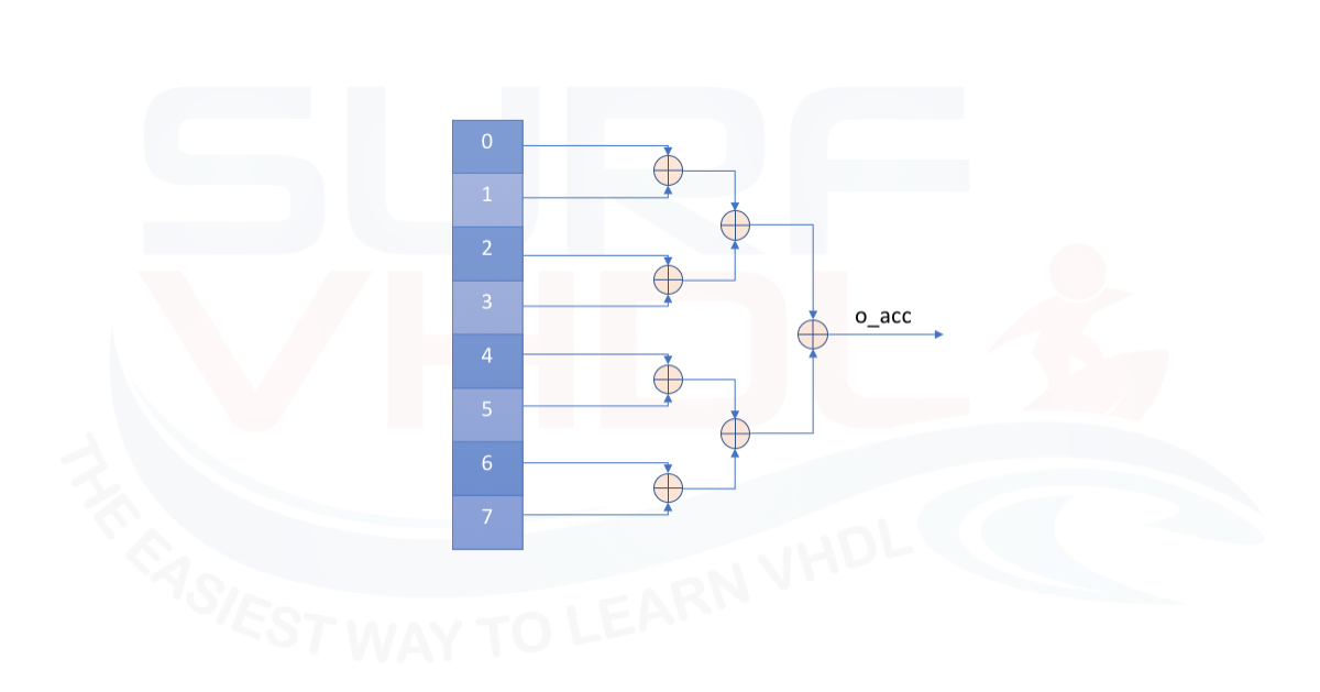
A more optimized architecture of the adder for the 8 values is represented in Figure 4.
In this case, the VHDL code implements a cascade of balanced adder equalizing the delay over the adder structure. A possible VHDL code description using FOR-LOOP approach of the adder cascade is given below
library IEEE;
use IEEE.std_logic_1164.all;
use IEEE.numeric_std.all;

entity accumulator_better is
port(
  i_clk             : in  std_logic;
  i_data0           : in  std_logic_vector(7 downto 0);
  i_data1           : in  std_logic_vector(7 downto 0);
  i_data2           : in  std_logic_vector(7 downto 0);
  i_data3           : in  std_logic_vector(7 downto 0);
  i_data4           : in  std_logic_vector(7 downto 0);
  i_data5           : in  std_logic_vector(7 downto 0);
  i_data6           : in  std_logic_vector(7 downto 0);
  i_data7           : in  std_logic_vector(7 downto 0);
  o_acc             : out std_logic_vector(10 downto 0));
end accumulator_better;

architecture rtl of accumulator_better is
constant C_NUMDATA    : integer := 8;
type t_data  is array (0 to C_NUMDATA-1) of signed(10 downto 0);
signal r_data            : t_data;

begin

p_accumulator_better : process (i_clk)
type t_data_temp4  is array (0 to (C_NUMDATA/2)-1) of signed(10 downto 0); -- 4
type t_data_temp2  is array (0 to (C_NUMDATA/4)-1) of signed(10 downto 0); -- 2
variable vacc4              : t_data_temp4;
variable vacc2              : t_data_temp2;
begin
  if rising_edge(i_clk) then
    r_data(0)  <= to_signed(to_integer(signed(i_data0)),11);
    r_data(1)  <= to_signed(to_integer(signed(i_data1)),11);
    r_data(2)  <= to_signed(to_integer(signed(i_data2)),11);
    r_data(3)  <= to_signed(to_integer(signed(i_data3)),11);
    r_data(4)  <= to_signed(to_integer(signed(i_data4)),11);
    r_data(5)  <= to_signed(to_integer(signed(i_data5)),11);
    r_data(6)  <= to_signed(to_integer(signed(i_data6)),11);
    r_data(7)  <= to_signed(to_integer(signed(i_data7)),11);

    l_acc4 : for k in 0 to (C_NUMDATA/2)-1 loop
      vacc4(k) := r_data(2*k) + r_data(2*k+1);
    end loop l_acc4;

    l_acc2 : for k in 0 to (C_NUMDATA/4)-1 loop
      vacc2(k) := vacc4(2*k) + vacc4(2*k+1);
    end loop l_acc2;

    o_acc <= std_logic_vector(vacc2(0) + vacc2(1));
  end if;
end process p_accumulator_better;

end rtl;
VHDL code accumulator using FOR-LOOP with balanced adder tree optimization
Layout consideration on FOR LOOP
Some consideration should be done on the VHDL code above.
If we try to layout either the parity check VHDL code or the accumulator VHDL code the VHDL synthesize can optimize our code implementing the best hardware structure for the device we are using.
Altera/Intel Implementation
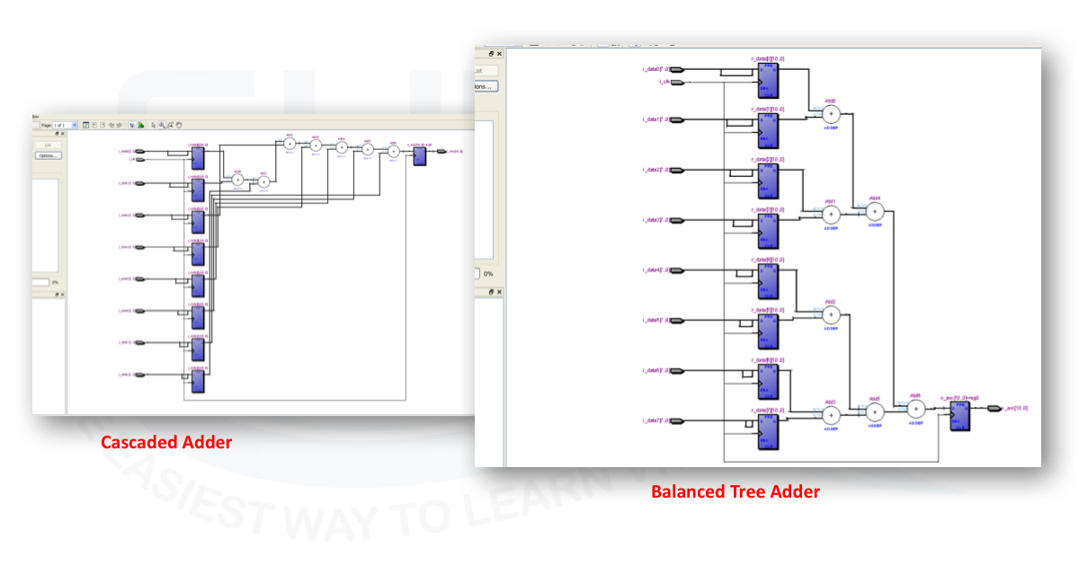
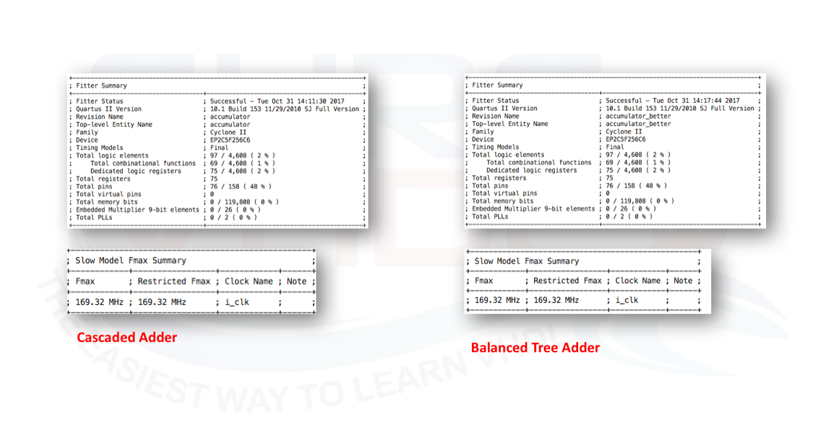
Altera Quartus II implements the different VHDL description of the adder in the same way. As clear from Figure 5, the RTL viewer reports different implementation for the VHDL code of cascaded adder or balanced tree adder.
In the first case, the adder tree is not balanced, in the second case the addition is performed using a balance adder tree.
In both cases, the Fitter and netlist optimizer implements on an Altera/Intel Cyclone II the same hardware mapping as clear from the fitter report and timing analysis in Figure 6.
Xilinx ISE Implementation
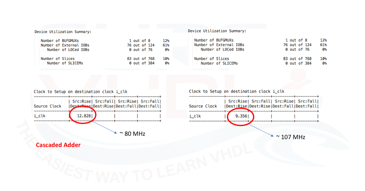
Xilinx ISE implements the different VHDL description of the adder in a slightly different way and the implementation depends on the VHDL RTL code. The FOR-LOOP implementation triggers different hardware architecture. A timing and area report for the two design is reported in
As clear, on a Xilinx Spartan 3 FPGA, equivalent to the Cyclone II Altera FPGA, the area and timing report for the two-different implementation differs both on area and timing. The maximum timing achievable is in the balanced VHDL code version and it is about 80 MHz in the cascaded adder implementation and about 107 MHz in the balanced tree adder implementation.
Xilinx vs Altera
In this particular example, Altera Quartus II optimization seems to work better than Xilinx ISE optimization.
It is always a good VHDL design approach to read the layout report such as mapper, fitter and static timing analysis in order to verify if the obtained results are in line with the expected ones.
Conclusion
In this post, we treated the implementation of FOR-LOOP in VHDL. After the VHDL syntax of the FOR-LOOP and its BNF, we tried to understand, in two different examples, the consideration to take into account when dealing with FOR-LOOP VHDL statement.
Last, but not least, the same VHDL code could be translated in different implementation by different synthesizer as we confirmed using Altera Quartus II and Xilinx ISE .
As a design rule, we should write a VHDL code that reflects the hardware architecture we want to realize in order to guide the VHDL synthesizer versus our hardware implementation.
Even if the synthesis software is becoming more and more powerful, we should always check the synthesis and mapping results to verify in our VHDL code has been translated as we expect.
Reference
[1] RTL HARDWARE DESIGN USING VHDL Coding for Efficiency, Portability, and Scalability
[2] VHDL Programming by Example 4th Ed Douglas – Perry
[4] Xilinx ISE
There is no good in using this expression: “to_signed(to_integer(signed(i_data0)),11)” other then resizing to 11 bits. So please don’t use casting with integer as an intermediate type. Integer is restricted to only 32 bits in almost all tools! You can simply write “resize(signed(i_data0), 11)”
Thank you for your feedback, Patrick!
hi master
i have been started FPGA with VHDL ago and i wanna start implemenation interface with FPGA.can you guidance me how start?
thank so much.
Which kind of project do you want to realize?
vacc4() is array with 4 length and 11 width , in line 47 ,vacc2(k) := vacc4(2*k) + vacc4(2*k+1) ;
i dont understand this line because the vacc4() is array with 4 length and 11 width
in other hand have 4 regiester with 11 bit width but suppose k=2 then vacc2(2) := vacc4(4) + vacc4(5) ;
What is the value of these two, vacc4(4) and vacc4(5)?
vacc4(4) is the element 5 of the array, each element is composed by 11 bit type unsigned,
the same for vacc4(5), is the 6-th element of the array.
Remember that array starts from 0.
iam from signal processing background,i was basically doing project based on FPGA and VHDL side ,i wanna learn VHDL language ,which is the best procedure to learn VHDL ,pls suggest
you can start from my course
https://surf-vhdl.teachable.com
Are they always loop structures synthesizable?
it depends. Not all the VHDL you can write is synthesizable. The same considerations are valid the loop structure
Hello,
I am trying to write a demultiplexer using the loop statement in ISE.
The traditional way:
…..
case sel_adrs is
when x”00″ <= demux_data <= input(0); –input(0) is array of slv and demux_data is slv
when x"01" <= demux_data demux_data <= input(i);
end loop demux_data;
The above gave a lot of errors. Please guide
The code gives you a lot of error because contains syntactic error 🙂
take a look here
http://surf-vhdl.com/vhdl-case-statement/
Hi
I need to implement the following paper
“FPGA based hardware implementation of Bat Algorithm”.
How can I do it?
BAT algorithm is quite complex.
You need to decompose the algorithm hierarchically.
Implement and simulate the single entities. Then integrate each block in a top level and…
good luck 🙂
Hi,
I would like to implement optimization algorithms in FPGA, how can I do it?