In this post, you will learn how to write the VHDL code for a full adder. Many years ago when you need to implement an arithmetic operator such as sum subtraction or multiplication, you had to design it by hand. Modern synthesis tools implement basic of arithmetic using the optimized library. This means that you don’t care about the implementation of the adder in the silicon device, i.e. ASIC or FPGA, you can use simply “+” operator to implement your full adder. Moreover, FPGA vendors such as ALTERA or XILINX provide you a macro generator for the arithmetic operator if you need custom behavior i.e. pipelining to speed up timing performances.
The NUMERIC_STD package
Since 1995, IEEE defines numeric types and arithmetic functions in the standard package ”numeric_std” to outline a standard approach for use arithmetic operator with synthesis tools.
Two numeric types are defined:
- UNSIGNED: represents an UNSIGNED number in vector form
- SIGNED: represents a SIGNED number in vector form
The base element type is type STD_LOGIC.
The leftmost bit is treated as the most significant bit.
Signed vectors are represented in two’s complement form.
The “numeric_std” package contains overloaded arithmetic operators on the SIGNED and UNSIGNED types. The package also contains useful type conversions functions.
Other packages, before this standardization, were defined by Synopsys:
- ieee.std_logic_arith
- ieee.std_logic_unsigned
- ieee.std_logic_signed
that despite the prefix “ieee” are not standard but Synopsys proprietary.
It is worth of notice that these packages are recognized by the most synthesis tool. In any case, it will be a good VHDL design approach to use standard library “ieee.numeric_std.all” especially is you start new VHDL design.
Full Adder VHDL entity
As you know, when you add two numbers of “N” bit, the results can be “N+1” bit wide. If you handle this increment of dynamics, you are implementing a full adder. If no dynamic increase is handled the adder implementation is simpler than the full adder one but the result can be wrapped around the “N” bit. Generally, if you know that no wrap around will occur, you can use a simple half-adder.
In this post, you can find out more about binary number representation and wrap around concept.
Here below is reported an example of full adder parametric entity. In the VHDL code, the full adder is implemented in line 24 on the registered input. Pay attention that before performing the addition operation you must extend the number of bit of the input operand. This is implemented using the standard “resize” function provided in the “numeric_std” package as in line 31 and 32.
library ieee;
use ieee.std_logic_1164.all;
use ieee.numeric_std.all;

entity adder_full_signed_reg is
generic(
  N             : integer := 8);
port (
  i_clk       : in     std_logic;
  i_add1      : in     std_logic_vector(N-1 downto 0);
  i_add2      : in     std_logic_vector(N-1 downto 0);
  o_sum       : out    std_logic_vector(N downto 0));
end adder_full_signed_reg;

architecture rtl of adder_full_signed_reg is

signal r_add1   : signed(N downto 0);
signal r_add2   : signed(N downto 0);
signal w_sum    : signed(N downto 0);

begin

-- combinatorial adder
  w_sum <= r_add1 + r_add2;

r_process : process(i_clk)
begin
  if(rising_edge(i_clk)) then

  -- register input and extend sign
    r_add1      <=  resize(signed(i_add1),N+1);
    r_add2      <=  resize(signed(i_add2),N+1);

  -- register output
    o_sum       <= std_logic_vector(w_sum);

  end if;
end process r_process;

end rtl;
In the example is implemented a signed full adder, if you need an unsigned full adder you need to replace the line containing “signed” data type definition with “unsigned” data type.
A simple example is given in the following bunch of VHDL code:
library ieee;
use ieee.std_logic_1164.all;
use ieee.numeric_std.all;

entity adder_full_unsigned is
generic(
  N        : integer := 8);
port (
  add1     : in     std_logic_vector(N-1 downto 0);
  add2     : in     std_logic_vector(N-1 downto 0);
  sum      : out    std_logic_vector(N downto 0));
end adder_full_unsigned;

architecture rtl of adder_full_unsigned is

begin

  sum <= std_logic_vector( resize(unsigned(add1),N+1) + resize(unsigned(add2),N+1) );

end rtl;
in this case, the adder is purely combinatorial.
Full adder trial layout
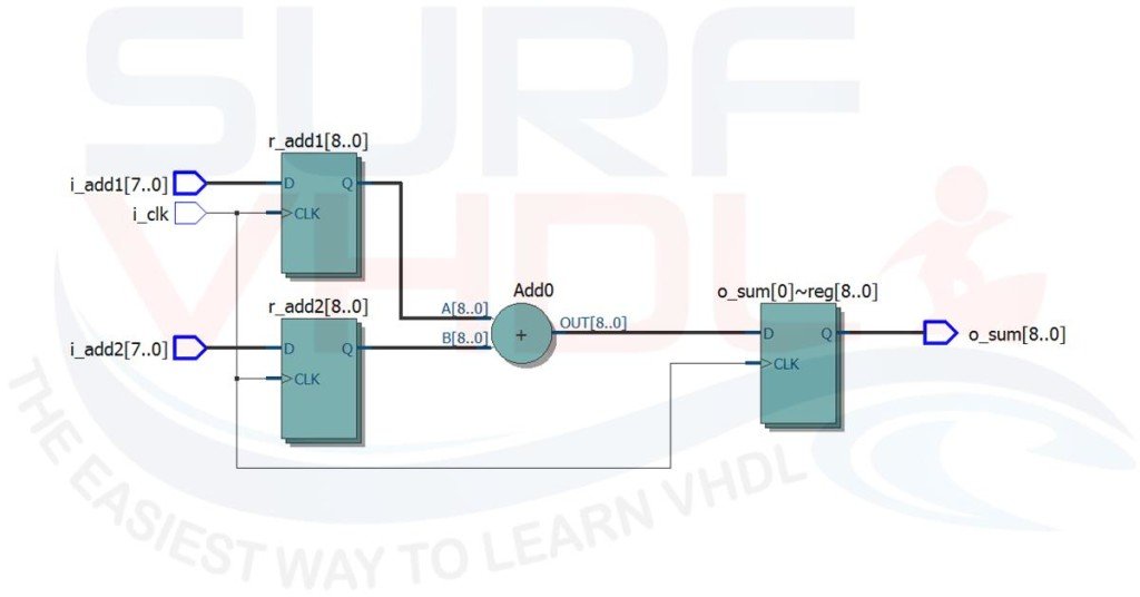
In Figure1 is reported a trial layout on ALTERA Quartus II using a Cyclone V FPGA. The signed full adder VHDL code presented above is pure VHDL RTL code so you can use it independently on every kind of FPGA or ASIC.
In Figure1 Quartus II implement sign extension on input operand, then add them and registers the output result as described in the VHDL code.

You can implement different size of adder just changing the input generic value on “N” that represents the number of bit of the full adder.
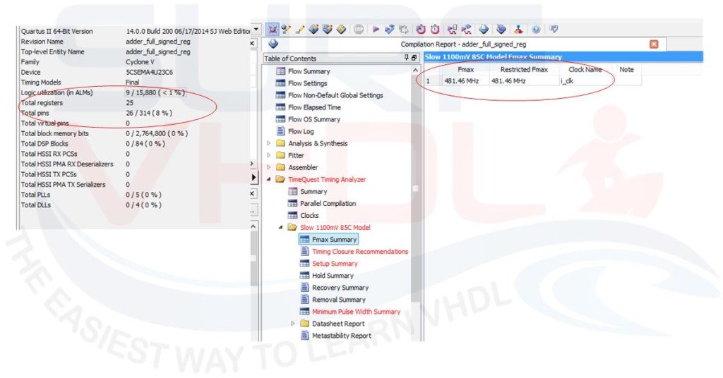
Figure2 reports the post-layout result:

Where you can notice that the number of registers used is 25: 8 for r_add1; 8 for r_add2; 9 for o_sum
the design runs at about 480 MHz.
VHDL code for Half Adder
If you don’t need to increment the dynamic you can use a half adder instead of a full adder.
library ieee;
use ieee.std_logic_1164.all;
use ieee.numeric_std.all;

entity adder_half_unsigned_reg is
generic(
  N       : integer := 256);
port (
  i_clk     : in     std_logic;
  i_add1    : in     std_logic_vector(N-1 downto 0);
  i_add2    : in     std_logic_vector(N-1 downto 0);
  o_sum     : out    std_logic_vector(N-1 downto 0));
end adder_half_unsigned_reg;

architecture rtl of adder_half_unsigned_reg is

signal r_add1    : unsigned(N-1 downto 0);
signal r_add2    : unsigned(N-1 downto 0);
signal w_sum     : unsigned(N-1 downto 0);

begin

-- combinatorial adder
  w_sum <= r_add1 + r_add2;

r_process : process(i_clk)
begin
  if(rising_edge(i_clk)) then

  -- register input
    r_add1      <=  unsigned(i_add1);
    r_add2      <=  unsigned(i_add2);

  -- register output
    o_sum       <= std_logic_vector(w_sum);

  end if;
end process r_process;

end rtl;
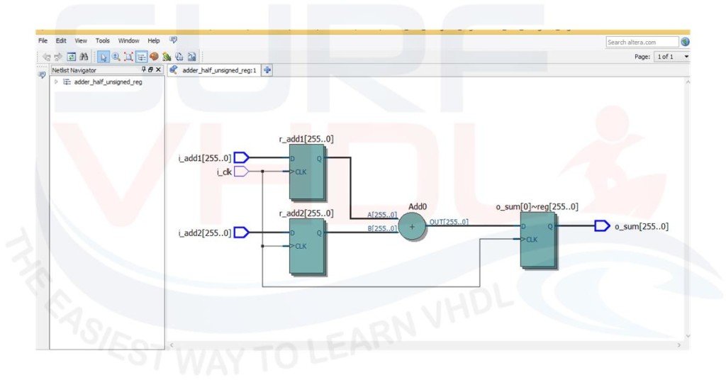
In Figure3 is reported the half-adder implementation where the number of input bit is 256. In this case, it is implemented a 256 bit full adder.

The FPGA is Cyclone V. In this example all the pins are mapped on I/O. it is not a realistic situation. This is only an example to understand how to implement a parametric adder VHDL code on FPGA.
library ieee;
use ieee.std_logic_1164.all;
use ieee.numeric_std.all;

entity test_adder_half_unsigned_reg is
generic(
  N          : integer := 256);
port(
  i_clk      : in     std_logic;
  o_sum      : out    std_logic_vector(N-1 downto 0));
end test_adder_half_unsigned_reg;

architecture rtl of test_adder_half_unsigned_reg is

component adder_half_unsigned_reg
generic(
  N        : integer := 256);
port (
  i_clk     : in     std_logic;
  i_add1    : in     std_logic_vector(N-1 downto 0);
  i_add2    : in     std_logic_vector(N-1 downto 0);
  o_sum     : out    std_logic_vector(N-1 downto 0));
end component;

signal r_add1     : std_logic_vector(N-1 downto 0);
signal r_add2     : std_logic_vector(N-1 downto 0);

begin

input_process : process(i_clk)
begin
  if(rising_edge(i_clk)) then

  -- register input
    r_add1      <=  std_logic_vector(signed(r_add1) + 1);
    r_add2      <=  std_logic_vector(signed(r_add2) - 1);

  end if;
end process input_process;

u_adder_half_unsigned_reg : adder_half_unsigned_reg
generic map(
  N         => N)
port map(
  i_clk       => i_clk   ,
  i_add1      => r_add1  ,
  i_add2      => r_add2  ,
  o_sum       => o_sum   );

end rtl;
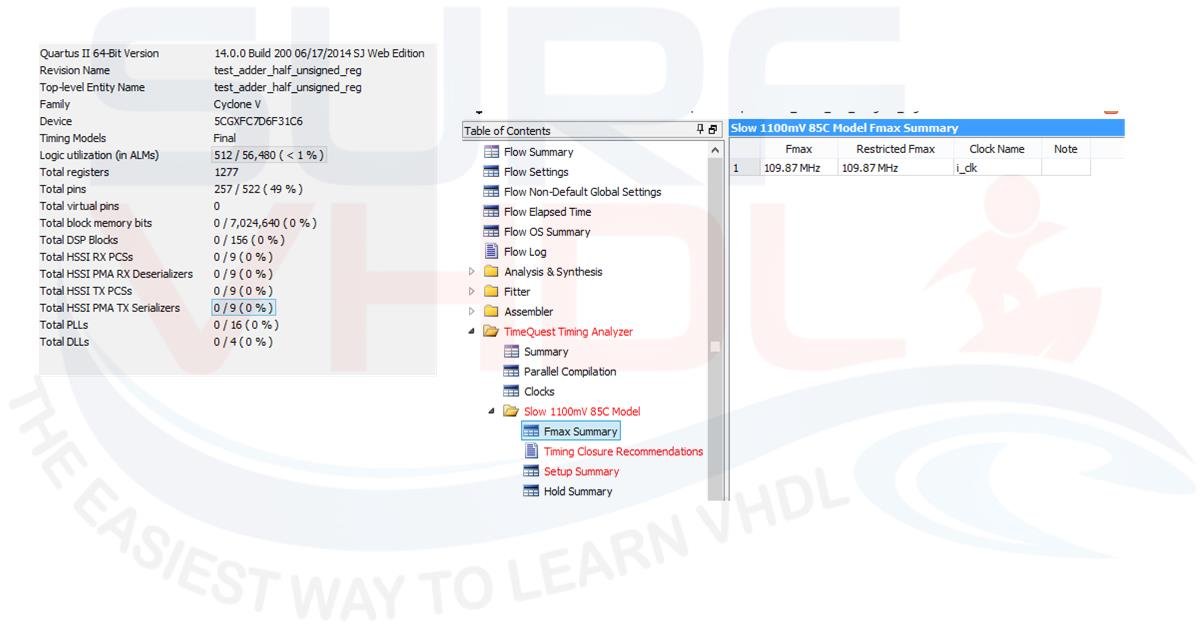
In order to layout the example, a test_adder_half_unsigned_reg container instantiate the adder_half_unsigned_reg generating two fake input to the component. This, of course, implements additional logic into the FPGA, but it is not important. Our purpose is to verify that the parametric design of half-adder with 256 bit dynamic can fit into the FPGA. As clear from the post-layout timing report of Figure4, the design can run up to about 110 MHz. Of course, in this case, the number of registers relative to the half adder is 256×3 = 768 over a total of 1277. The other flip-flops are used to implement the test bench that instantiates the half-adder.

As you see, the layout tool, Quartus II in this example, is smart enough to implement adder logic even for large input operands.
If the requirements in terms of timing are demanding, a pipeline implementation is required. For example, cascading 4-full-adder of 64 bit with proper carry bit handling.
If you appreciated this post, please help us to share it with your friend.
[social_sharing style=”style-7″ fb_like_url=”https://surf-vhdl.com/how-to-implement-a-full-adder-in-vhdl” fb_color=”light” fb_lang=”en_US” fb_text=”like” fb_button_text=”Share” tw_lang=”en” tw_url=”https://surf-vhdl.com/how-to-implement-a-full-adder-in-vhdl” tw_button_text=”Share” g_url=”https://surf-vhdl.com/how-to-implement-a-full-adder-in-vhdl” g_lang=”en-GB” g_button_text=”Share” linkedin_url=”https://surf-vhdl.com/how-to-implement-a-full-adder-in-vhdl” linkedin_lang=”en_US” alignment=”center”]
If you need to contact us, please write to: surf.vhdl@gmail.com
We appreciate any of your comment, please post below:
Though the implementation of larger logic diagrams is possible with the above full adder logic a simpler symbol is mostly used to represent the operation. Given below is a simpler schematic representation of a one-bit full adder.
sir i am designing a low pass fir filter but i am stuck with the code. can u please help me out by sending the code and the explanation of the code
you can implement a low pass filter using a FIR filter.
If you can use matlab just use “FDATOOL”, then you can use this post as example for implementing the VHDL code
The text is talking about half adders (HAs) and full adders (FAs). Non of you code listings is correct and shows the implementation of a FA or HA. Your code shows 2 different N-bit ripply carry adders (RCAs).
whats the next post?
Hi, if you need to know something just let me know
ciao
Copied and pasted in the Max Pluss II. Didn’t work.
The error was in the compilation section. “TDF syntax error”
Help me please.
which code did you copy and paste?
hi,
i want to design and implement in FPGA a controller for a new hoverboard. the controller will be implemented in the FPGA fabric and designed to drive the motor in 3 speeds: the 95%, 50% and 10% of the maximum speeds. do you think you can help me out with guidelines on writing the codes. thanks.
hi, maybe the best solution is a microcontroller. Why do you want to use an FPGA?
Hello
I’m a newbie and very beginner in FPGA. I have a question regarding with FPGA and Microcontoller uses in digital electronic system. For what system/cases that is better to use FPGA and in other case we should use microcontroller?
Thank you
This is a question that cannot be answered in a comment.
Basically if you can do it with a microcontroller, it is better to use a microcontroller.
FPGA should be used when you have real-time requirement that cannot be achieved or are difficult to achieve using microcontroller.
BTW, I will write a post on it.
Thank you for the question
Ciao
I see the resize takes care of the potential overflow, so that can be used with multiply also –
I was thinking of a condition where
Uvalue, an unsigned number is multiplied by Svalue a signed 2’C number, which is then assigned to Zvalue or Zvalue = Svalue* Uvalue.
hello
i want to design 4 bit full adder(signed and unsigned)
also i need testbench for that vhdl code
could you help me?