Implement a Digital Delay Using a Dual Port Ram
The digital delay lines are one of the most used blocks in the digital design. When the digital delay is small in terms of numbers of Flip-Flop a simple shift register approach can be used. If the number of bits to delay i.e. the number of Flip-Flop utilized became important, a different approach should be used.
In this post, a FIFO delay approach has been presented. In that case, we used the FIFO macro provided by the FPGA vendor in order to implement a digital delay line.
Digital Delay as Circular Buffer
The basic approach is to use a RAM block as storing element acting on write and read pointer to address the delay. This is also, the basic approach of FIFO architecture:
- Memory block
- Write pointer
- Read pointer
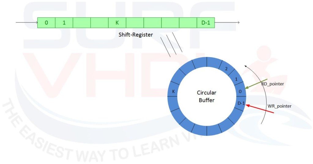
The memory block acts as a circular buffer. In this case, no “shift” is implemented on the incoming data.
The delay is controlled by write and read pointer as in Figure1
When the system starts, the write pointer will be incremented by one until the number of input data written into memory is equal to the delay required. From this moment on, data is read out from memory and input data is stored into memory incrementing both write and read pointer.
The write – read pointer offset is equal to the required delay.
VHDL Implementation of Digital Delay as Circular Buffer
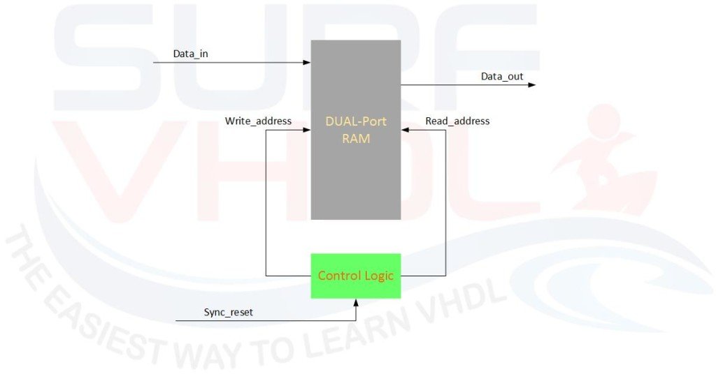
The architecture of a digital delay line implemented using dual port RAM is highlighted in Figure2. An example of VHDL code implementation of the architecture proposed in Figure2 is reported below. Note that the dual port RAM is implemented directly in VHDL/RTL. This VHDL code is technology independent for what concerns FPGA approach implementation.
library IEEE;
use IEEE.std_logic_1164.all;
use IEEE.numeric_std.all;

entity delay_line is
generic(
  W                 : integer := 8;    -- data width
  L                 : integer := 1200);  -- delay length, shall be > 3
port(
  i_clk             : in  std_logic;
  i_sync_reset      : in  std_logic;
  i_data            : in  std_logic_vector(W-1 downto 0);
  o_data            : out std_logic_vector(W-1 downto 0));
end delay_line;

architecture rtl of delay_line is

type t_ram is array (L-2 downto 0) of std_logic_vector(W-1 downto 0);
signal m_ram : t_ram;

signal r_addr_wr         : integer range 0 to L-2;
signal r_addr_rd         : integer range 0 to L-2;
signal r_enable_read     : std_logic;

begin

p_write : process (i_clk)
begin
  if rising_edge(i_clk) then
    if(i_sync_reset='1') then
      r_addr_wr      <= 0;
      r_enable_read  <= '0';
    else
      m_ram(r_addr_wr) <= i_data;
      if(r_addr_wr<L-2) then
        r_addr_wr      <= r_addr_wr + 1;
      else
        r_addr_wr      <= 0;
        r_enable_read  <= '1';       -- enable reading section
      end if;
    end if;
  end if;
end process p_write;

p_read : process (i_clk)
begin
  if rising_edge(i_clk) then
    if(i_sync_reset='1') then
      r_addr_rd      <= 0;
    else
      if(r_enable_read='1') then
        o_data         <= m_ram(r_addr_rd) ; -- additional delay
        if(r_addr_rd<L-2) then
          r_addr_rd      <= r_addr_rd + 1;
        else
          r_addr_rd      <= 0;
        end if;
      end if;
    end if;
  end if;
end process p_read;


end rtl;
You should check the area report in order to verify that the dual port RAM RTL/VHDL code infers eventually the dual port RAM block macro of your FPGA. The Quartus RTL viewer infers a dual port ram on the signal “m_ram“.
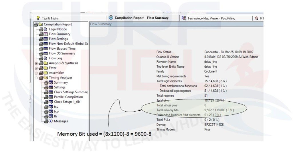
You should notice that the memory bits used in the report are:
(8 x 1200) – 8 = 9600-8 = 9592
In the RTL code of the digital delay implementation using RAM, line 52 adds an additional delay at the output register “o_data“. This register is used in order to guarantee a good performance in terms of timing delay (static timing analysis).
Here below is reported an example of a layout using Altera Cyclone II FPGA. As clear from the Altera Quartus II report, the VHDL code of the delay line is implemented on a Block RAM.
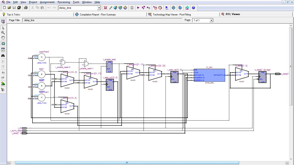
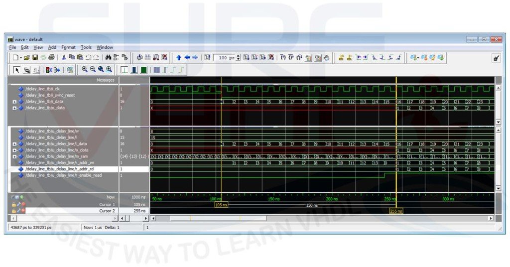
Figure5 shows the simulation of the RTL code of digital delay where the digital delay length is set to 15. The clock cycle is 10 ns. The delay between input and output data is 150 ns.
Note for ASIC implementation
Pay attention if you want to use this bunch of VHDL code for digital delay line on ASIC technology. In this case, as you know the ASIC technology implements dual port RAM as proprietary MACRO. Generally, you cannot infer dual port RAM macro as VHDL/RTL code in ASIC technology. The solution is to instantiate a dual port RAM Macro as a component inside your code.
If you appreciated this post, please help us to share it with your friend.
[social_sharing style=”style-7″ fb_like_url=”https://surf-vhdl.com/how-to-implement-a-digital-delay-using-a-dual-port-ram” fb_color=”light” fb_lang=”en_US” fb_text=”like” fb_button_text=”Share” tw_lang=”en” tw_url=”https://surf-vhdl.com/how-to-implement-a-digital-delay-using-a-dual-port-ram” tw_button_text=”Share” g_url=”https://surf-vhdl.com/how-to-implement-a-digital-delay-using-a-dual-port-ram” g_lang=”en-GB” g_button_text=”Share” linkedin_url=”https://surf-vhdl.com/how-to-implement-a-digital-delay-using-a-dual-port-ram” linkedin_lang=”en_US” alignment=”center”]
If you need to contact us, please write to: surf.vhdl@gmail.com
We appreciate any of your comment, please post below:
Wonderful web site. Plenty of helpful information here.
I am sending it to some pals ans additionally sharing in delicious.
Annd naturally, thank you to your sweat!
Thank You!
Can I suggest removing the read address counter? The write address counter yields the same values and read enable blocks any reads until the second pass anyway.