
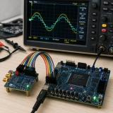
What is an Analog-to-Digital Converter (ADC)?
ADCs translate analog electrical signals, usually the voltage amplitude, into a sequence of discrete values (integer number) for data processing purposes. The bit resolution of the analog to digital conversion determines the magnitude of the quantization error. The number of discrete levels depends on the number of ADC bit resolution. For an N-bit ADC, the number of discrete possible values is 2^N.
For example, for an 8-bit ADC the input signal is discretized in 2^8 = 256 different values.
You can find a complete description of ADC here:
https://en.wikipedia.org/wiki/Analog-to-digital_converter
There are a wide number of ADC vendors. Here below you can check for the best ADC for your design:
Figure 1 shows the ADC transfer function: the analog input voltage referred to the Full-Scale Range (FSR) vs. the digital output ADC code. In the example, a 3-bit ADC is taken into account.
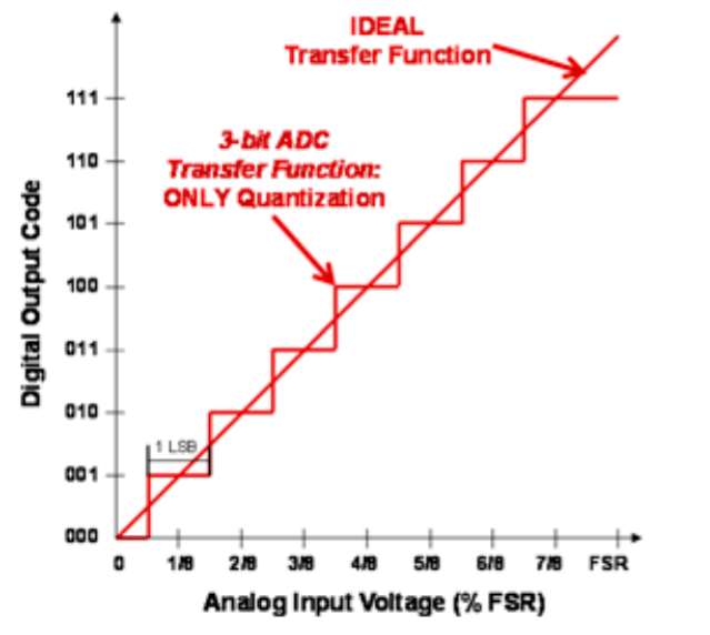
Figure 1 – ADC conversion transfer function
Principal ADC Digital Interfaces
The principal ADC digital interfaces are:
- Parallel Single Data Rate (SDR)
- Parallel Double Data Rate (DDR)
- Serial interface I2C, SPI
- Serialized LVDS interface
- JESD204A / JESD204B serial interface. You can find out more at www.jedec.org
Parallel interfaces are typically used for high-speed ADCs (> 1 MSPS).
Serial SPI or I2C interfaces are used for low-speed ADCs (< 10 MSPS). If you are working with these devices, you can read our dedicated post on how to connect a serial ADC to an FPGA.
The JEDEC standard for ADC JESD204A high-speed serial interface reduces board routing requirements and lowers pin count requirements for the receiving device.
An example of a JEDEC ADC is the TI ADC12J1600 12-Bit, 1.6 GSPS RF sampling ADC with JESD204B interface or the Analog Devices AD9690 14-Bit, 500 MSPS / 1 GSPS JESD204B, Analog-to-Digital Converter.
ADC-FPGA Interfacing Basics
In this post, we cover the basics of ADC interfacing, starting with the parallel Single Data Rate (SDR) interface.
In this example, we will refer to the Texas Instruments ADC ADS5542 14-Bit, 80 MSPS Analog-to-Digital Converter. This ADC implements a simple parallel output interface to output the digital data from the device.
The component in the example is summarized in Figure 2.
On the left side is represented the differential analog input clock and analog input data.
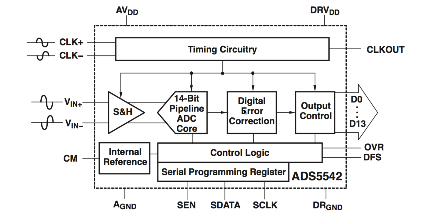
Figure 2 – ADS5542 internal architecture
On the right side, the digital output clock (“CLKOUT”) is used to clock the converted data (D0–D13) of the ADC. In the timing diagram of Figure 3, the ADC provides output converted data on the falling clock output edge. It is possible to program the ADC to provide data on the output clock rising edge. For further information, you can check the ADC datasheet here.
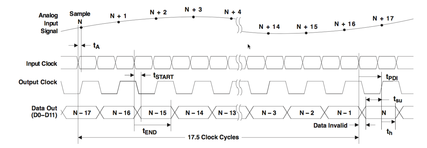
Figure 3 – ADS5542 conversion timing
Single Data Rate (SDR) Interfacing Example
At this point let’s see how to interface an ADC with a Single Data Rate (SDR) parallel output to an FPGA. Our hypothesis is to have a timing diagram like Figure 3 above, i.e., the ADC digital data is present at the ADC output interface on the rising edge of the ADC digital clock. Under this condition, the best clock edge should be the rising edge of the ADC “output clock”. This is true if the input delay of clock and data is the same. In Figure 4, Dly1 = Dly2.
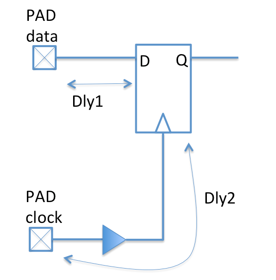
Figure 4 – FPGA Data vs Clock delay
If Dly1 – Dly2 = clock period / 2, the best clocking edge will be the falling edge.
In order to guarantee optimum sampling, a simple trick is to foresee the clock sampling swap at the FPGA ADC input interface and to set the input flip-flop inside the FPGA pad if allowed by the technology.
While the VHDL code handles the logic, keep in mind that ensuring robust setup and hold times at the physical pins requires defining proper timing constraints in your SDC file (e.g., using set_input_delay).
The following simple VHDL example can be used to sample ADC data at the FPGA input. This example is customized for a 4-bit input strictly to simplify the RTL and Technology Map viewer examples.
library ieee;
use ieee.std_logic_1164.all;

entity adc_parallel_interface is
port (
  i_clk      : in  std_logic;
  i_rstb     : in  std_logic;
  i_data     : in  std_logic_vector(3 downto 0);
  o_data     : out std_logic_vector(3 downto 0));
end adc_parallel_interface;

architecture rtl of adc_parallel_interface is

signal r_data   : std_logic_vector(3 downto 0);

begin

p_adc_parallel_interface : process(i_clk,i_rstb)
begin
  if(i_rstb='0') then
    r_data              <= (others=>'0');
    o_data              <= (others=>'0');
  elsif(rising_edge(i_clk)) then
    r_data              <= i_data;
    o_data              <= r_data;
  end if;
end process p_adc_parallel_interface;

end rtl;
The RTL viewer of Quartus II in Figure 5 reports the four-bit input and output registers.
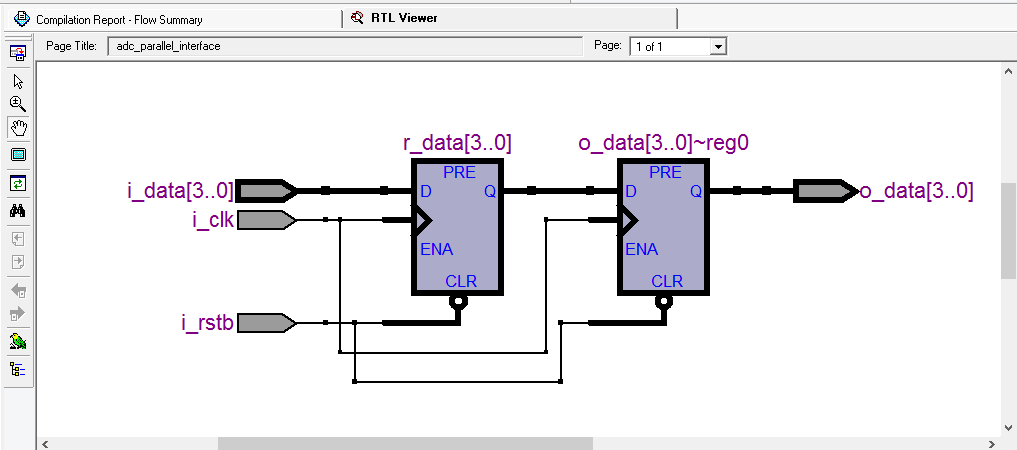
Figure 5 – Quartus II RTL viewer for FPGA-ADC SDR interfacing
In the technology MAP viewer, the input and output pad buffers are reported.
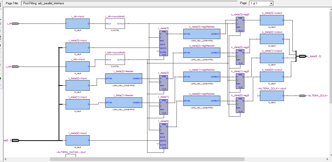
Figure 6 – Quartus II MAP viewer for FPGA-ADC SDR interfacing
Mapping Input/Output Registers to the FPGA Pad
Most FPGA technologies allow mapping input and output registers directly on the FPGA pad. The input and output register mapping should be enabled using their custom setting.
In Quartus II, it is possible to enable mapping input and output registers using the “Pin Planner” window or adding the following constraints in a TCL script file:
For output register mapping:
set_instance_assignment -name FAST_OUTPUT_REGISTER ON -to o_data[3]
set_instance_assignment -name FAST_OUTPUT_REGISTER ON -to o_data[2]
set_instance_assignment -name FAST_OUTPUT_REGISTER ON -to o_data[0]
set_instance_assignment -name FAST_OUTPUT_REGISTER ON -to o_data[1]
For input register mapping:
set_instance_assignment -name FAST_INPUT_REGISTER ON -to i_data[3]
set_instance_assignment -name FAST_INPUT_REGISTER ON -to i_data[2]
set_instance_assignment -name FAST_INPUT_REGISTER ON -to i_data[1]
You can also use wildcards:
set_instance_assignment -name FAST_OUTPUT_REGISTER ON -to o_data[*]
set_instance_assignment -name FAST_INPUT_REGISTER ON -to i_data[*]
Note: Although the screenshots and assignment examples reference Quartus II and Cyclone III, the VHDL code and the underlying I/O pad logic apply identically to modern toolchains like Intel Quartus Prime or Xilinx Vivado.
Double Data Rate (DDR) Interfacing Example
The following VHDL code can be used to sample input ADC data using the rising and falling clock edge. The signal i_rise_fall_b is used to select the clock edge to be used.
library ieee;
use ieee.std_logic_1164.all;

entity adc_parallel_interface_ddr is
port (
  i_clk            : in  std_logic;
  i_rise_fall_b    : in  std_logic;
  i_data           : in  std_logic_vector(3 downto 0);
  o_data           : out std_logic_vector(3 downto 0));
end adc_parallel_interface_ddr;

architecture rtl of adc_parallel_interface_ddr is

signal r_data_rise      : std_logic_vector(3 downto 0);
signal r_data_fall      : std_logic_vector(3 downto 0);

begin

p_sample_rise : process(i_clk)  -- sample ADC data on rising edge
begin
  if(rising_edge(i_clk)) then
    r_data_rise              <= i_data;
  end if;
end process p_sample_rise;

p_sample_fall : process(i_clk) -- sample ADC data on falling edge
begin
  if(falling_edge(i_clk)) then
    r_data_fall              <= i_data;
  end if;
end process p_sample_fall;

p_output : process(i_clk)  -- select EDGE sampling
begin
  if(rising_edge(i_clk)) then
    if(i_rise_fall_b='1') then
      o_data              <= r_data_rise;
    else
      o_data              <= r_data_fall;
    end if;
  end if;
end process p_output;

end rtl;
The RTL viewer in Figure 7 shows the mux used to select between the rising and falling edge.
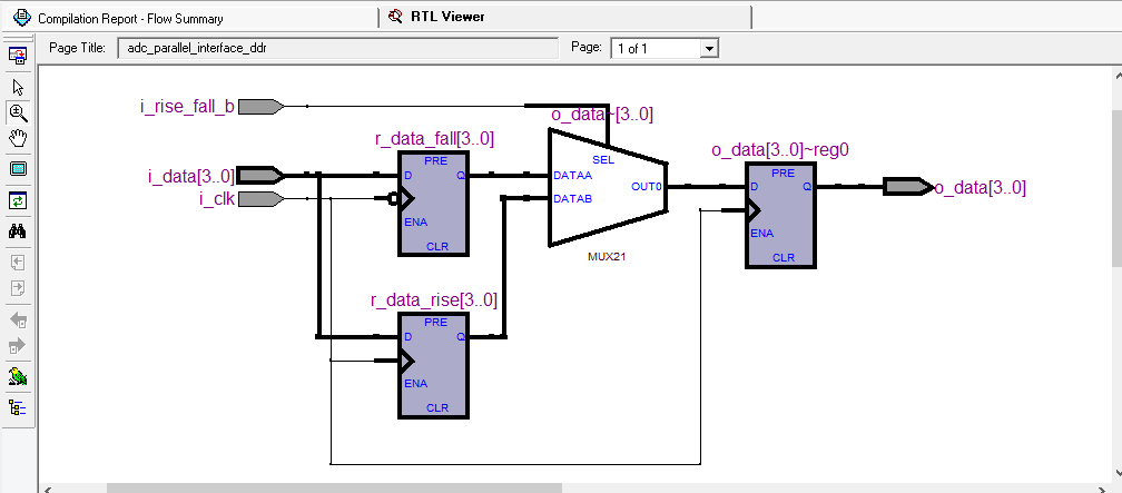
Figure 7 – Quartus II RTL viewer for FPGA-ADC DDR interfacing
The Technology Map viewer in Figure 8 also shows a logic cell used as a mux.
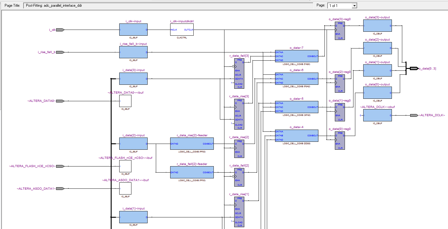
Figure 8 – Quartus II MAP viewer for FPGA-ADC DDR interfacing
Many FPGAs have the capability of Double Data Rate (DDR) sampling, i.e., the ability to use both rising and falling clock edges directly inside the FPGA PAD.
For the Cyclone III FPGA used in this example, the input/output flip-flop and the mux are implemented inside the FPGA PAD using dedicated resources as in Figure 9.
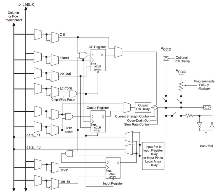
Figure 9 – Cyclone III – PAD Architecture
Figure 10 reports the input DDR buffer architecture of Cyclone III.
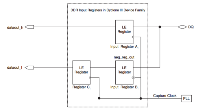
Figure 10 – Cyclone III – Input Buffer Architecture
As is clear, the DDR input is de-muxed in dataout_h and dataout_l.
How Much ADC Sampled Data Can You Store in an FPGA?
Many ADC evaluation boards contain an FPGA on board connected to the ADC. The FPGA is used to acquire ADC sampled data in order to evaluate the ADC performances. Clearly, the quantity of ADC sampled data that can be stored depends on the installed FPGA and the memory available on the evaluation board (EVB).
Let’s see some examples to clarify this issue.
Suppose we have an ADC connected to an FPGA. A possible simplified architecture is in Figure 11.
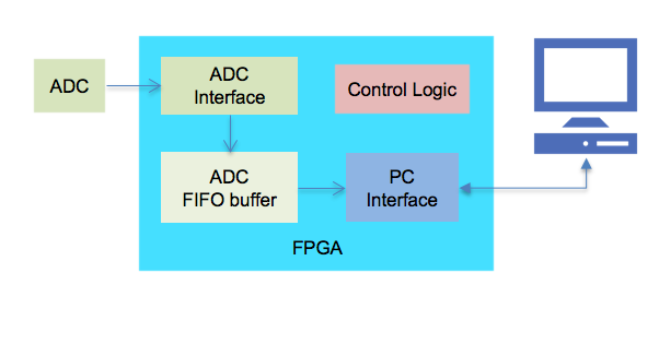
Figure 11 – ADC-FPGA interfacing and acquisition
The ADC is a 10-bit ADC and the FPGA is a Cyclone III EP3C16 shown in Figure 12.
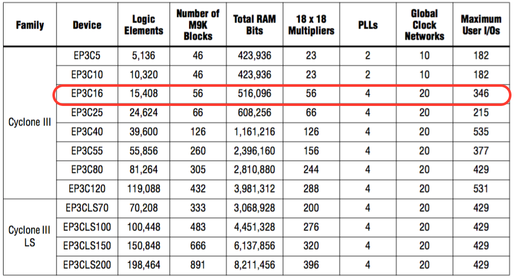
Figure 12 – Cyclone III FPGA family overview
The FPGA implements 516096 bits of internal RAM, so the maximum storage available is equal to the FPGA available RAM.
For a 10-bit ADC, we can store up to:
516096 / 10 = 51609 ADC words (rounded down to the nearest integer)
Each ADC word contains 10 bits. Going deep into the FPGA architecture, the FPGA RAM is implemented using M9K memory blocks; in the selected FPGA there are up to 56 memory blocks available. The Altera M9K blocks support the following features:
- 8,192 memory bits per block (9,216 bits per block including parity)
- Independent read-enable (rden) and write-enable (wren) signals for each port
- Packed mode in which the M9K memory block is split into two 4.5 K single-port RAMs
- Variable port configurations
- Single-port and simple dual-port modes support for all port widths
- True dual-port (one read and one write, two reads, or two writes) operation
- Byte enables for data input masking during writes
- Two clock-enable control signals for each port (port A and port B)
- Initialization file to pre-load memory content in RAM and ROM modes
The block can be configured as:
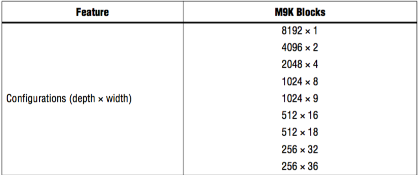
Table 1 – Altera M9K memory block configuration
So now we can review the number of ADC 10-bit words we can store inside the EP3C16 FPGA memory. The memory buffer must be quantized as reported in the memory block configuration, so let’s compute the storing efficiency for each configuration.
Total memory blocks = 56.
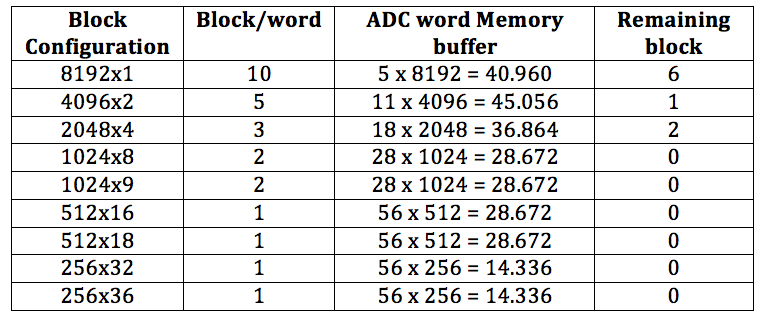
Table 2 – ADC-FPGA interface maximum storage selection
The best memory configuration is achieved using 4096×2 configuration (see Table 2) that uses all the M9K blocks but one with the higher efficiency. Remember that M9K is a memory block of 8192 + 1024 = 9216 bits.
The last step is to compute how long the acquisition can be.
In this case, we need to know the ADC sampling frequency.
The acquisition time is:
Tacq = Memory Buffer (words) / ADC Speed (MSamples/sec)
The ADS5542 can sample data up to 80 MSPS. So at maximum sampling rate we can store up to:
45.056 / 80.000.000 = 563.2 µs
(The 45.056 value comes from the best configuration in Table 2: 4096 × 11 blocks = 45.056 words.)
Conclusion and Next Steps
Interfacing an ADC to an FPGA comes down to managing timing requirements and properly utilizing the physical I/O resources of the device. While parallel interfaces like SDR and DDR are the standard choice for high-speed sampling, many designs rely on serial interfaces to drastically reduce pin count.
If your project requires a serial protocol (such as SPI), fill out the form below to download the complete VHDL example code for connecting a serial ADC to an FPGA.
How to Connect an ADC to an FPGA
Get the complete VHDL code from this article.