

Introduction to ASK modulation
In this post, we are going to understand the fundamentals of Digital Modulation from the basics. An example of VHDL implementation of a digital modulator is given at the end of the post.
Digital Modulation technique is very important in the telecommunication world and substituted the analog modulation since it is more flexible and can be implemented with small and cheap electronics. We will focus on the implementation of the digital modulator.
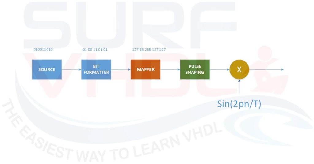
Figure 1 – Example of digital modulator Architecture
Amplitude-shift keying (ASK) is a form of amplitude modulation that represents digital data as variations in the amplitude of a carrier wave.
For example, the transmission of the binary symbol ‘1’ can be represented by transmitting a fixed-amplitude carrier wave and fixed frequency for a bit duration of T seconds (bit rate). If the signal value is ‘1’ then the carrier signal will be transmitted; otherwise, a signal value of ‘0’ will be transmitted.
Like AM, an ASK is also linear and very sensitive to atmospheric noise, distortions, propagation conditions so the efficiency in terms of Signal-to-Noise ratio is very low. The ASK modulation and demodulation processes are relatively inexpensive. The ASK technique is also commonly used to transmit digital data over optical fiber.
More general, ASK can be used to transmit a finite number of amplitudes, each assigned a unique pattern of binary digits. Usually, each amplitude encodes an equal number of bits.
For example, if we decide to encode 2 bits per symbol transmitted, the amplitudes transmitted are:
00 => A0
01 => A1
10 => A2
11 => A3
Of course, increasing the number of different transmitted amplitude (the number of bits we transmit for each symbol), the required Signal-to-Noise ratio increases.
ASK modulator architecture
A typical architecture of a modulator is reported in Figure 1
From the left:
- Digital source
- Bit-formatter
- Mapper
- Low-pass interpolator shaping filter
- Optional Up-converter
The low-pass interpolator shaping filter smooths the transitions between discrete amplitude levels, reducing out-of-band emissions and improving spectral efficiency. It is optional in simplified implementations but essential for meeting spectral mask requirements in practical communication systems.
The interactive example above shows the full ASK modulator chain with 12 pseudo-random 2-bit meta-symbols and a ×8 upsampling rate. Row ① displays the meta-symbol sequence (00, 01, 10, 11). Row ② compares the raw mapper output (dashed) with the shaped amplitude after the low-pass filter (solid purple). Row ③ shows the RF modulated signal with 4 carrier cycles per symbol period, demonstrating how the amplitude envelope follows the shaped output.
The digital source can be either internal or external and provides the serial bit-stream to be transmitted at bit rate Rb. The serial bit-stream is “packetized” into a meta-symbol of two or more bits, two bits in this example. The output frequency of the meta-symbols is Rb/Np, where Np is the number of bits of the meta-symbol. The meta symbols are mapped following the desired modulation scheme.
For ASK example, the input symbol is mapped to an N-bit discrete amplitude.
In this post, we will focus on the mapper using 2 bits for the input meta-symbol and 8 bits for mapper output.
The timing relationship between the serial bit stream and the meta-symbol is as follows: every Np bits from the serial stream are grouped into one meta-symbol. At a bit rate of Rb, the meta-symbol rate is Rb/Np. Each meta-symbol is held for one meta-symbol period, during which the mapper outputs a constant amplitude level.
VHDL implementation of ASK mapper
The mapper can receive a 2-bit input i.e. four different meta symbols value:
- 00
- 01
- 10
- 11
The meta-symbol will be mapped into an 8-bit amplitude. The mapping scheme can be decided to maximize the channel efficiency. In this example, we will map the 4 values into 4 different equally distributed intervals. For 8 bit mapping, the possible values are 0, 1, .. 255. Dividing the interval 0..255 in 4 we get 256/4 = 64
- 00 => 63
- 01=> 127
- 10 => 191
- 11 => 255
A possible VHDL code implementation is given below:
library ieee;
use ieee.std_logic_1164.all;
use ieee.numeric_std.all;

entity mapper_ask is
port (
  i_clk                       : in  std_logic;
  i_rstb                      : in  std_logic;
  i_meta_sym                  : in  std_logic_vector(1 downto 0);
  o_mapper                    : out std_logic_vector(7 downto 0));
end mapper_ask;

architecture rtl of mapper_ask is
type t_mapper_table is array(0 to 3) of integer range 0 to 255;
constant mapper_table              : t_mapper_table := (
   63,
  127,
  191,
  255);

signal r_meta_sym                  : integer range 0 to 3; -- used as mapper_table pointer

begin

p_mapper_ask : process(i_clk,i_rstb)
begin
  if(i_rstb='0') then
    r_meta_sym        <= 0;
    o_mapper          <= (others=>'0');
  elsif(rising_edge(i_clk)) then
    r_meta_sym        <= to_integer(unsigned(i_meta_sym));
    o_mapper          <= std_logic_vector(to_unsigned(mapper_table(r_meta_sym),8));
  end if;
end process p_mapper_ask;

end rtl;
VHDL Code for the ASK mapper
The output pattern is stored in the LUT “mapper_table”. If you need different or programmable mapping pattern the solution can be:
- Use an internal dual-port RAM
- Use a set of registers
The dual port RAM approach is adopted when the number of mapper symbols is huge (greater than 8 – 10 or more), the register is used otherwise.
In Figure 2 is reported a simulation of the mapper behavior when the input meta-symbol is cycling 0,1,2,3,0,…
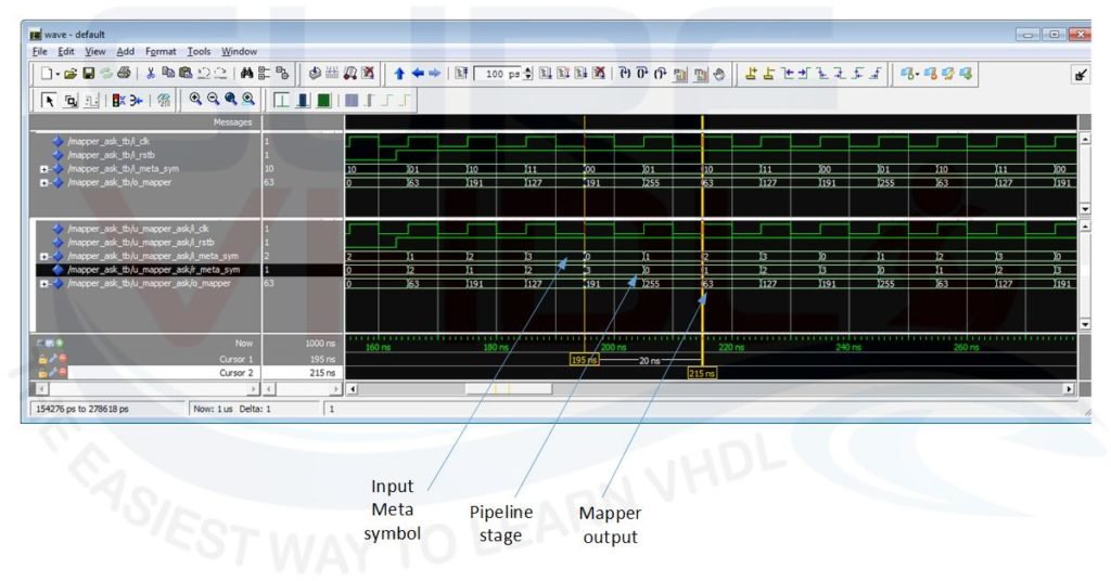
Figure 2 – ModelSim Mapper simulation
Simplified implementation of ASK modulator
In Figure 3 is shown a simplified architecture of an ASK modulator. In the architecture, no shaping filter is present. The modulator is implemented using a Mapper, and up-converter. The up-conversion is implemented by multiplying the mapper output with a digital generated sine waveform. In the example, we will use the dds_sine sine waveform generator implemented in this post. The DDS is configured with a 32-bit phase accumulator and a 14-bit sine output. The carrier frequency is set via the 32-bit frequency control word (i_fcw) and the optional start phase (i_start_phase). For a system clock of 50 MHz, a wide range of carrier frequencies can be generated with fine resolution.
The simplified ASK modulator above cycles through the 4 symbols (00 → 01 → 10 → 11 → …), showing the carrier amplitude changing with each symbol value. No shaping filter is applied: the amplitude jumps instantly between levels.
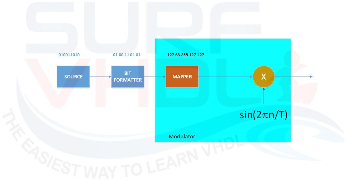
Figure 3 – ASK Modulator simplified architecture
The VHDL code of ASK modulator multiplies the mapper output by sine wave generated by dds_sine in the process “p_mapper_ask_simple”. When you multiply two integer number of N and M bit, the result is N+M bits. In this case, the mapper output is 8 bit unsigned, so if we want to multiply two numbers, the first signed (sine wave) by the second unsigned (the mapper output) we need to add the sign bit to the unsigned number. Of course, the sign bit will be zero because the mapper output is always positive. In this case, the result will be N+M+1 as in line 66 of the VHDL code for the modulator below.
library ieee;
use ieee.std_logic_1164.all;
use ieee.numeric_std.all;

entity modulator_ask_simple is
port (
  i_clk                       : in  std_logic;
  i_rstb                      : in  std_logic;
  i_sync_reset                : in  std_logic;
  i_fcw                       : in  std_logic_vector(31 downto 0);
  i_start_phase               : in  std_logic_vector(31 downto 0);
  i_meta_sym                  : in  std_logic_vector( 1 downto 0);
  o_molulator                 : out std_logic_vector(11 downto 0));
end modulator_ask_simple;

architecture rtl of modulator_ask_simple is

component mapper_ask
port (
  i_clk                       : in  std_logic;
  i_rstb                      : in  std_logic;
  i_meta_sym                  : in  std_logic_vector(1 downto 0);
  o_mapper                    : out std_logic_vector(7 downto 0));
end component;

component dds_sine
port(
  i_clk          : in  std_logic;
  i_rstb         : in  std_logic;
  i_sync_reset   : in  std_logic;
  i_fcw          : in  std_logic_vector(31 downto 0);
  i_start_phase  : in  std_logic_vector(31 downto 0);
  o_sine         : out std_logic_vector(13 downto 0));
end component;

signal w_sine                      : std_logic_vector(13 downto 0);
signal w_mapper                    : std_logic_vector( 7 downto 0);
signal r_molulator                 : signed(11 downto 0);
signal r_upconverted               : signed(22 downto 0); -- 14 + 8 + 1 bit sign always '0'

begin
o_molulator     <= std_logic_vector(r_molulator);

u_mapper_ask : mapper_ask
port map(
  i_clk                       => i_clk                       ,
  i_rstb                      => i_rstb                      ,
  i_meta_sym                  => i_meta_sym                  ,
  o_mapper                    => w_mapper                    );

u_dds_sine : dds_sine
port map(
  i_clk          => i_clk          ,
  i_rstb         => i_rstb         ,
  i_sync_reset   => i_sync_reset   ,
  i_fcw          => i_fcw          ,
  i_start_phase  => i_start_phase  ,
  o_sine         => w_sine         );

p_modulator_ask_simple : process(i_clk,i_rstb)
begin
  if(i_rstb='0') then
    r_upconverted          <= (others=>'0');
    r_molulator            <= (others=>'0');
  elsif(rising_edge(i_clk)) then
    r_upconverted          <= signed(w_sine) * signed('0'&w_mapper);
    -- 12 MSB; bit 22 and bit 21 are always the same
    r_molulator            <= r_upconverted(21 downto 10);
  end if;
end process p_modulator_ask_simple;

end rtl;
VHDL code for a simplified ASK modulator
Since the modulator output is 12 bits, we take the most significant bits of the multiplication result. The mapper output is 8-bit unsigned; to multiply it with the 14-bit signed sine wave, we zero-extend the mapper to 9 bits by prepending a ‘0’ sign bit. This extra sign bit is always ‘0’, so the two most significant bits (bit 22 and bit 21) of the 23-bit result are identical.
Therefore we select bits 21 down to 10 (12 bits) instead of 22 down to 11, as shown in line 68. The simulation in Figure 4 confirms that bit 22 and bit 21 of the “r_upconverted” signal are always equal.
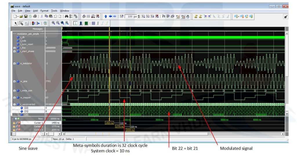
Figure 4 – ASK Modulator simulation
Layout on FPGA
In Figure 5 is reported the layout report of the modulator implemented above. The FPGA is the Cyclone III present in the Altera DE0 board. As clear from the report the modulator uses the internal RAM to implement the sine wave for the up-conversion and the resource required are low: less than 1% of the (small) FPGA. The working frequency is about 200 MHz.
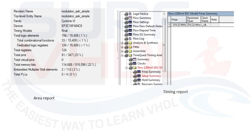
Figure 5 – ASK Modulator FPGA layout report on Cyclone III EP3C16F484C6.
Conclusion
In this post, we developed a simple ASK modulator in VHDL. The VHDL code example for the modulator has been simulated and implemented in a Cyclone III Altera FPGA. You can use this baseline to implement your custom digital modulator in VHDL.
Implement Digital ASK Modulator in VHDL
Get the complete VHDL code from this article.
Reference
[1] Digital Modulation in Communications Systems — An Introduction
[2] Understanding Modern Digital Modulation Techniques
[3] Introduction to Digital Modulation