
Often, inside our FPGA design, we need to generate a local clock from the system clock. By system clock, I mean the clock that comes from an external board oscillator. Many modern FPGAs have the capability to generate internal clocks, different from the external clocks, using internal PLL hard macros. So you can generate an internal FPGA clock as a multiple or sub-multiple of the external system clock.
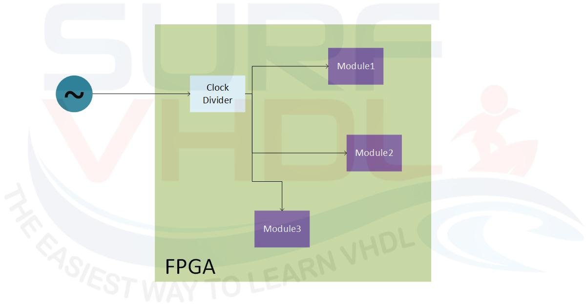
Figure1 – FPGA with internal clock divider
Sometimes PLLs are used to modify the clock phase or to generate different clocks at the same frequency with different phase relationships. For instance:
Clock1, clock2 and clock3 where:
- Clock1 is the reference clock
- Clock2 has 90° phase offset
- Clock3 has 180° phase offset
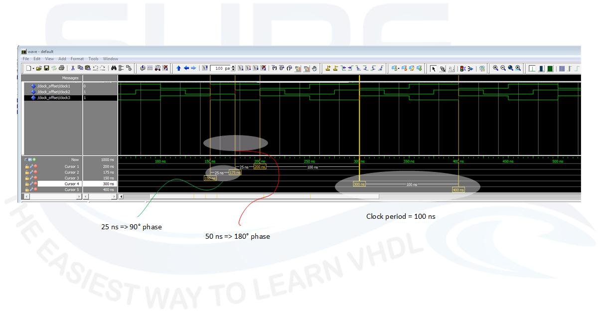
Figure2 – Clock Offset Example
- Clock1 has a 100 ns period.
- Clock2 offset with respect to clock1 is 25 ns = 100 ns/4 (i.e. 90° ).
- Clock3 offset with respect to clock1 is 50 ns = 100 ns/2 (i.e. 180° ).
Method 1: Clock Division by Two
If the clock we need is simply the system clock divided by two, we can implement a simple divider using a flip-flop and inverter:
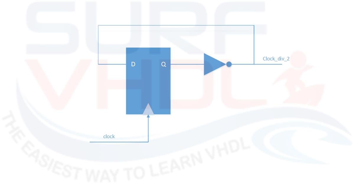
Figure3 – Clock divider by two example
This is the simplest clock divider you can implement into an FPGA or ASIC. Sometimes this approach is used to generate a clock with a 50% duty cycle even starting from a source clock that has a duty cycle different from 50%.
Figure4 shows an example where the source clock has a duty cycle of 34/66 and the divided clock has a duty cycle of 50%.
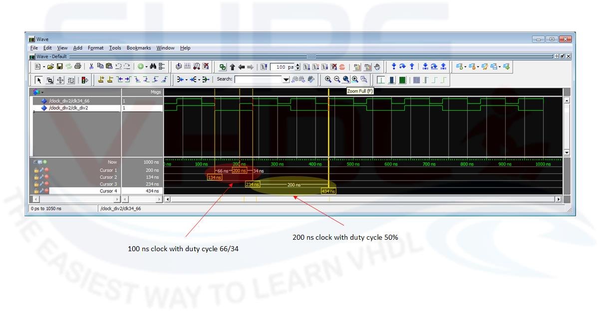
Figure4 – Clock divider by two simulation example
The VHDL code for a clock divider by 2 is:
signal clk34_66       : std_logic:='0';
signal clk_div2       : std_logic:='0';

begin

-- test clock generator
-- NOT synthesizable only for test
p_clk34_66 : process
begin
  clk34_66  <= '0';
  wait for 34 ns;
  clk34_66  <= '1';
  wait for 66 ns;
end process p_clk34_66;

-- divider by two: synthesizable VHDL code
p_clk_div2: process(clk34_66)
begin
  if(rising_edge(clk34_66)) then
    clk_div2   <= not clk_div2;
  end if;
end process p_clk_div2;
As you can see, it is a simple process that implements the flip-flop and inverter of Figure3.
Method 2: Clock Division by a Power of Two
If you generalize the clock divider by two, a smart and efficient divider is the clock divider by a power of two. This clock divider can be implemented using a free running simple wrap around counter as in Figure5.
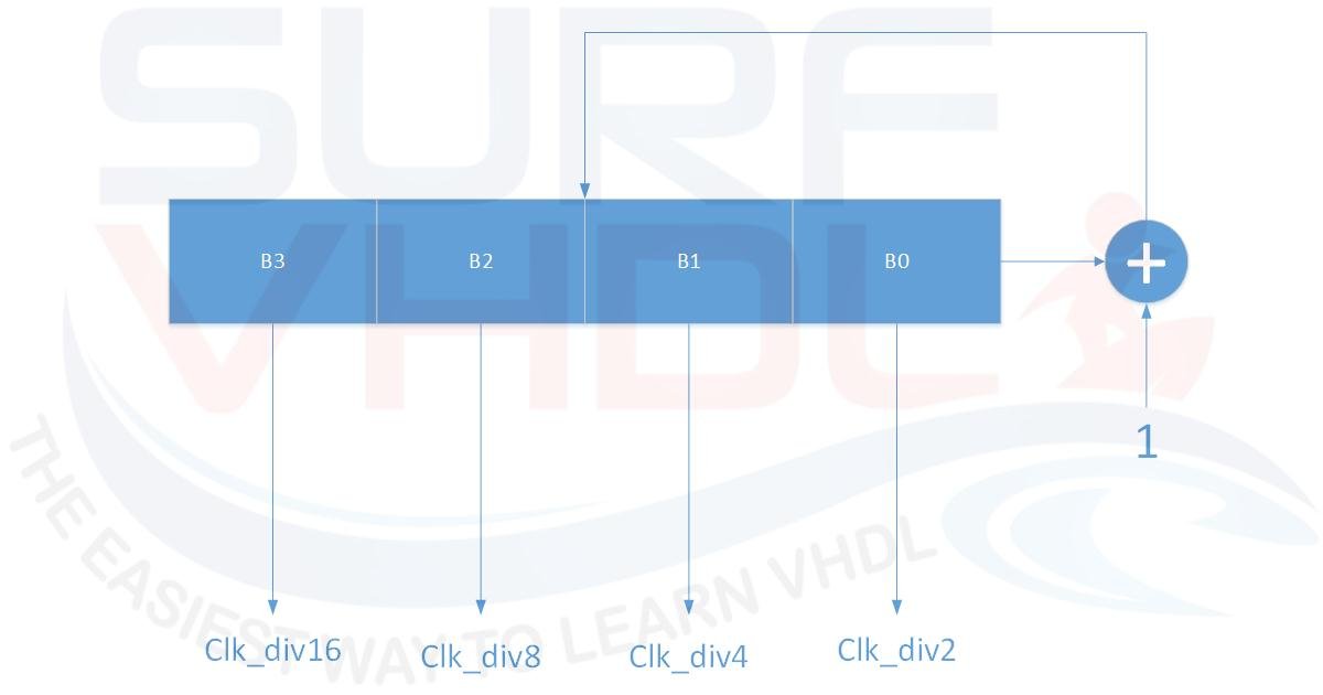
Figure5 – Clock Divider by a power of two Architecture example
You can think of the clock divider by two as a wraparound counter where the Least Significant Bit (LSB) is used to generate the clock. The counter LSB flips at half the clock rate, which means that it can be used as a clock divider by two.
What happens to the other bits?
The second bit, bit 1 (numbering LSB as bit 0), changes its state at half the rate of bit 0, so bit 1’s rate is ¼ of the clock rate. The bit k rate is 1/(2^(k+1)) of the clock rate.
For instance, bit 3 rate is:
1/(2^(3+1)) = 1/16
The VHDL for a clock divider by a power of two is very simple and straightforward as you can see in the example below.
library IEEE;
use IEEE.std_logic_1164.all;
use IEEE.numeric_std.all;

entity clock_div_pow2 is
port(
  i_clk         : in  std_logic;
  i_rst         : in  std_logic;
  o_clk_div2    : out std_logic;
  o_clk_div4    : out std_logic;
  o_clk_div8    : out std_logic;
  o_clk_div16   : out std_logic);
end clock_div_pow2;

architecture rtl of clock_div_pow2 is

signal clk_divider        : unsigned(3 downto 0);

begin


p_clk_divider: process(i_rst,i_clk)
begin
  if(i_rst='0') then
    clk_divider   <= (others=>'0');
  elsif(rising_edge(i_clk)) then
    clk_divider   <= clk_divider + 1;
  end if;
end process p_clk_divider;

o_clk_div2    <= clk_divider(0);
o_clk_div4    <= clk_divider(1);
o_clk_div8    <= clk_divider(2);
o_clk_div16   <= clk_divider(3);

end rtl;
In this VHDL code of the clock divider, we have introduced the asynchronous reset signal.
If you do not reset the clk_counter at a known state, the simulation doesn’t run.
It is a good design rule to reset the clock divider unless differently specified because you will start your clock divider state from a known condition. When implementing the divider without the reset signal, you must set the initial condition to the clk_counter signal during the declaration of the signal itself:
signal clk_counter : unsigned(3 downto 0):=(others=>'0');
Remember that this VHDL code is still synthesizable, so you can use it without any problem, but your clock divider start condition is unknown. The simulation of the VHDL code for the clock divider by a power of two is reported in Figure6.
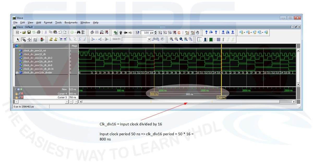
Figure6 – Clock Divider by a power of two Simulation
Method 3: Clock Division by an Integer
What if you need a derived clock that is an integer submultiple of your board clock?
Can we generalize the approach we saw above?
The answer is YES.
If we need a derived clock that is an integer submultiple of the source clock, we can still use a counter to divide the source clock, just counting how long the derived clock should stay high and how long it should stay low. Of course, when we state “how long”, this time is given in terms of source clock cycles.
A possible VHDL code implementation of an integer clock divider is given below.
library IEEE;
use IEEE.std_logic_1164.all;
use IEEE.numeric_std.all;

entity clock_div is
port(
  i_clk         : in  std_logic;
  i_rst         : in  std_logic;
  i_clk_divider : in  std_logic_vector(3 downto 0);
  o_clk         : out std_logic);
end clock_div;

architecture rtl of clock_div is

signal r_clk_counter        : unsigned(3 downto 0);
signal r_clk_divider        : unsigned(3 downto 0);
signal r_clk_divider_half   : unsigned(3 downto 0);

begin

p_clk_divider: process(i_rst,i_clk)
begin
  if(i_rst='0') then
    r_clk_counter       <= (others=>'0');
    r_clk_divider       <= (others=>'0');
    r_clk_divider_half  <= (others=>'0');
    o_clk               <= '0';
  elsif(rising_edge(i_clk)) then
    r_clk_divider       <= unsigned(i_clk_divider)-1;
    r_clk_divider_half  <= unsigned('0'&i_clk_divider(3 downto 1)); -- half
    if(r_clk_counter < r_clk_divider_half) then
      r_clk_counter   <= r_clk_counter + 1;
      o_clk           <= '0';
    elsif(r_clk_counter = r_clk_divider) then
      r_clk_counter   <= (others=>'0');
      o_clk           <= '1';
    else
      r_clk_counter   <= r_clk_counter + 1;
      o_clk           <= '1';
    end if;
  end if;
end process p_clk_divider;

end rtl;
In the VHDL example, the counter is used to count the number of source clock cycles we want the derived clock to stay high and stay low. As you can see, the clock division factor i_clk_divider is defined as an input port. The generated clock stays high for half the i_clk_divider cycles and low for half the i_clk_divider cycles.
- If i_clk_divider is even, the clock divider provides a divided clock with 50% duty cycle.
- If i_clk_divider is odd the duty cycle cannot be 50%.
In case i_clk_divider is odd, the duty cycle approaches 50% for higher division factors. For instance:
i_clk_divider = 3;  clock high = 2 cycles; clock low = 1 cycle;  duty ~33/66
i_clk_divider = 15; clock high = 8 cycles; clock low = 7 cycles; duty ~46/54
i_clk_divider = 6;  clock high = 3 cycles; clock low = 3 cycles; duty 50/50
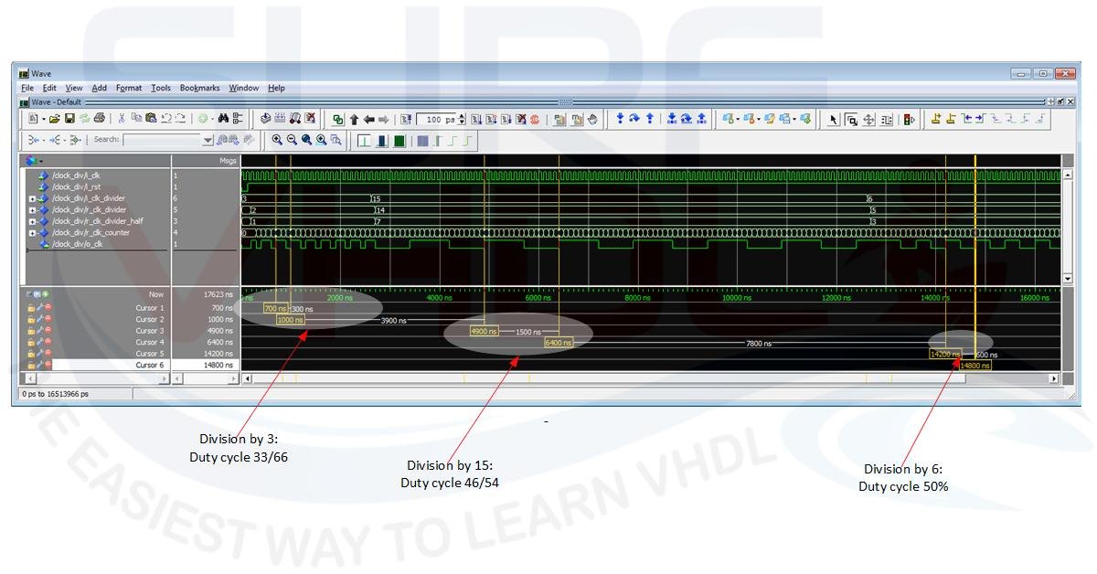
Figure7 – Clock Divider by integer simulation
Interactive Clock Divider Waveform
Adjust the slider to see how the division factor affects the derived clock.
Advanced Tip: Logic Clocks vs. Clock Enables (CE)
While dividing a clock using counters and flip-flops creates what is known as a logic clock, it is worth discussing why and when you might use this approach instead of a simple Clock Enable (CE) signal.
Usually, generating a CE pulse every N cycles is considered a standard best practice because it keeps the entire design synchronous to the main system clock. However, the purpose of clock division is often to relax timing requirements for specific parts of your logic that can afford to run at a lower speed.
If your main system clock is very fast, relying purely on a CE signal means the timing analyzer will still evaluate those paths at the high-speed clock rate. To tell the synthesis tool to relax the timing, you would need to apply complex multicycle path constraints. These constraints make timing verification tricky and are highly prone to errors if not managed perfectly.
In such scenarios, generating a divided logic clock can be a practical alternative to avoid complex timing constraints. By doing so, you allow that specific section of the circuit to naturally work at a relaxed pace. However, to do this safely, you must pay strict attention to how this new clock is distributed.
Best Practices: Clock Tree Handling and Buffers
This post received a lot of comments both on social channels and on this website. Many of these considerations are valid, since the post did not clarify how to handle the clock tree.
So let’s clarify this point better. When you use this kind of approach you must pay attention to how the layout tool “understands” this architecture. Specifically, you must check if the layout tool inserts a clock buffer at the root of your logic clock to avoid excessive loading on the line.
Generally, layout tools such as ISE, Vivado, or Quartus are smart enough and automatically insert clock buffers (like a BUFG) at the root of the clock tree, i.e., at the output of the clock divider module. You have to check if these buffers are present and provide the tool with the proper timing constraints. If no buffers are inserted automatically, you must instantiate them by hand in your VHDL code in order not to destroy the timing performance and stability of your design due to high fan-out routing delays.
If you use VHDL / RTL code for your clock divider you can easily port your VHDL code to different FPGAs or ASIC technologies. Using a PLL approach you need to tailor your code on different technology.
This approach can be used when you need to divide by an integer your clock and you don’t have the possibility or don’t want to instantiate a PLL / DCM inside the FPGA. A good reason for using this approach could be if you need to change “run-time” the clock division factor, for instance, to slow down the clock when you need to save power consumption. The integer clock divider allows you to reconfigure the clock frequency by simply setting the clock division factor.
When you deal with custom hard macro inside the FPGA i.e., transceiver, PCIe macro and so on, this approach cannot be used. In this case, the layout tool raises an error when the clock routing is not possible.
Conclusion
Implementing a clock divider in VHDL is a fundamental skill for any FPGA designer. Whether you need a simple division by two, a power of two, or an arbitrary integer, understanding how to construct these logic clocks using counters is essential.
Remember that while using a Clock Enable (CE) is the standard practice for synchronous design, a divided logic clock can be a powerful tool to naturally relax multicycle timing constraints in high-speed systems. Always pay close attention to your clock tree and ensure the synthesis tools correctly infer global clock buffers to maintain the integrity and performance of your design.