

When to Use a RAM Instead of a Shift Register
Digital delay lines are among the most used blocks in digital design. When the required digital delay is small in terms of the number of flip-flops, a simple shift register approach can be used. However, if the number of bits to delay, i.e., the number of flip-flops utilized becomes significant, a different approach should be adopted to save area and routing resources.
In a previous post, a FIFO delay approach was presented.
Circular Buffer Architecture for Digital Delays
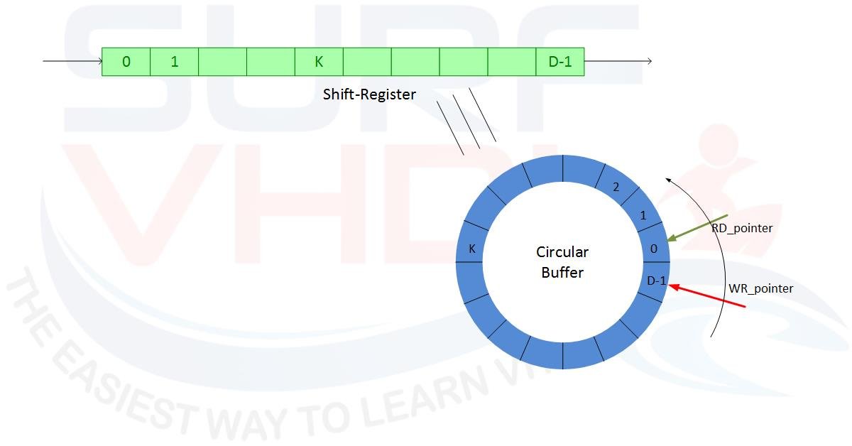
Figure 1 – Digital Delay Implementation Architecture as Circular Buffer
The basic approach is to use a RAM block as a storage element, relying on write and read pointers to address the delay. This is also the foundational concept of a FIFO architecture:
- Memory block
- Write pointer
- Read pointer
The memory block acts as a circular buffer. In this configuration, no “shift” is implemented on the incoming data.
The delay is controlled by the write and read pointers, as shown in Figure 1. When the system starts, the write pointer is incremented by one until the amount of input data written into memory equals the required delay. From this moment on, data is read out from the memory and new input data is stored, incrementing both the write and read pointers simultaneously.
The offset between the write and read pointers is exactly equal to the required delay.
VHDL Code Implementation
The architecture of a digital delay line implemented using a dual-port RAM is highlighted in Figure 2. An example of VHDL code implementing the architecture proposed in Figure 2 is shown below. Note that the dual-port RAM is implemented directly in VHDL/RTL. This VHDL code is technology-independent for FPGA implementations.
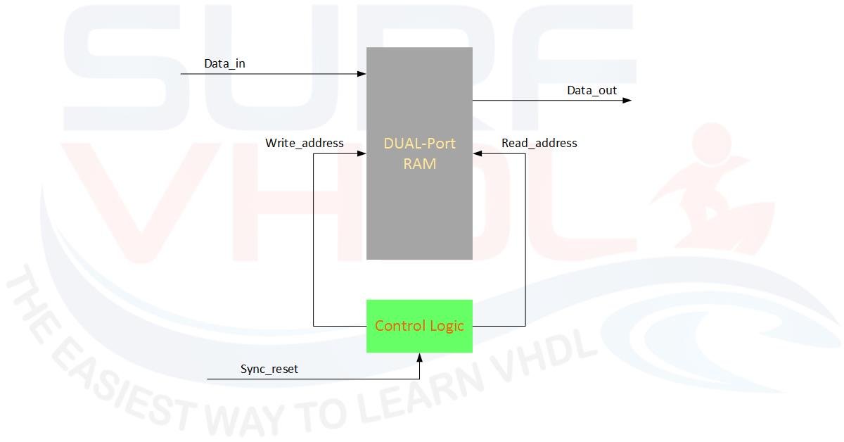
Figure2 – Architecture of Digital Delay Line using Dual Port RAM
library IEEE;
use IEEE.std_logic_1164.all;
use IEEE.numeric_std.all;

entity delay_line is
generic(
  W                 : integer := 8;    -- data width
  L                 : integer := 1200);  -- delay length, shall be > 3
port(
  i_clk             : in  std_logic;
  i_sync_reset      : in  std_logic;
  i_data            : in  std_logic_vector(W-1 downto 0);
  o_data            : out std_logic_vector(W-1 downto 0));
end delay_line;

architecture rtl of delay_line is

type t_ram is array (L-2 downto 0) of std_logic_vector(W-1 downto 0);
signal m_ram : t_ram;

signal r_addr_wr         : integer range 0 to L-2;
signal r_addr_rd         : integer range 0 to L-2;
signal r_enable_read     : std_logic;

begin

p_write : process (i_clk)
begin
  if rising_edge(i_clk) then
    if(i_sync_reset='1') then
      r_addr_wr      <= 0;
      r_enable_read  <= '0';
    else
      m_ram(r_addr_wr) <= i_data;
      if(r_addr_wr<L-2) then
        r_addr_wr      <= r_addr_wr + 1;
      else
        r_addr_wr      <= 0;
        r_enable_read  <= '1';       -- enable reading section
      end if;
    end if;
  end if;
end process p_write;

p_read : process (i_clk)
begin
  if rising_edge(i_clk) then
    if(i_sync_reset='1') then
      r_addr_rd      <= 0;
    else
      if(r_enable_read='1') then
        o_data         <= m_ram(r_addr_rd) ; -- additional delay
        if(r_addr_rd<L-2) then
          r_addr_rd      <= r_addr_rd + 1;
        else
          r_addr_rd      <= 0;
        end if;
      end if;
    end if;
  end if;
end process p_read;


end rtl;
Design Note on Reset Behavior: Notice that the i_sync_reset signal resets the pointers (r_addr_wr, r_addr_rd, and r_enable_read) but does not clear the contents of m_ram. This is intentional and necessary: FPGA Block RAMs typically do not support a global reset for their internal memory cells. If you attempt to reset the memory array inside the VHDL process, the synthesis tool will fail to infer a Block RAM and will implement the delay using thousands of individual logic registers instead.
Interactive Circular Buffer Simulator
To better understand how the read and write pointers behave cycle by cycle, you can interact with the simulator below. Click “Pulse Clock” to see how the circular buffer fills up and how the read pointer follows the write pointer to maintain the specified delay.
FPGA Synthesis: Block RAM Inference and Area
You should check the area report to verify that the VHDL code successfully infers the dual-port RAM block macro of your specific FPGA. The Quartus RTL viewer infers a dual-port RAM on the signal m_ram.
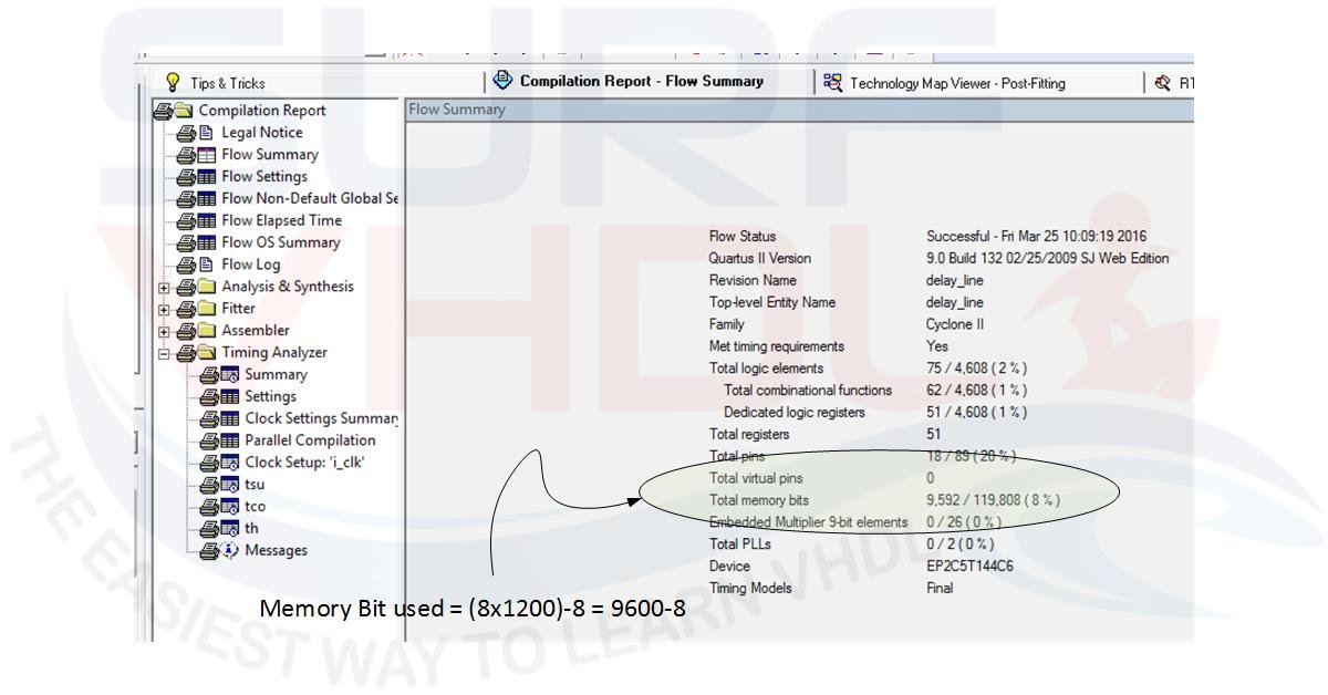
Figure3 – Quartus Area Report for VHDL code of Digital Delay Line with delay = 1200
You should notice that the memory bits used in the report are:
(8 x 1200) – 8 = 9600 – 8 = 9592
Why -8? The VHDL code defines the RAM array from L-2 downto 0, which equals 1199 memory locations of 8 bits each (1199 × 8 = 9592 bits). The remaining 8 bits required to reach the full delay length of 1200 are provided by the final output register o_data.
In the RTL code of the digital delay implementation using RAM, the output register o_data adds an additional delay. This register is used to guarantee optimal performance in terms of timing delay during static timing analysis.
Below is an example of a layout using an Altera Cyclone II FPGA. As is clear from the Altera Quartus II report, the VHDL code of the delay line is mapped directly onto a Block RAM.
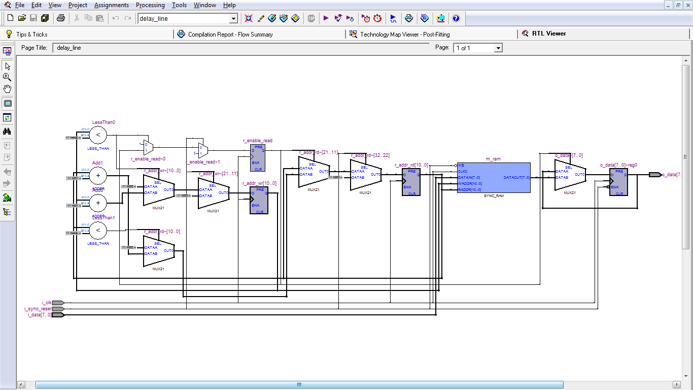
Figure4 – Quartus II RTL viewer for VHDL code of Digital Delay Line
RTL Simulation and Timing Analysis
Figure5 shows the Modelsim simulation of the RTL code, where the digital delay length is set to 15. The clock cycle is 10 ns. The resulting delay between input and output data is 150 ns.
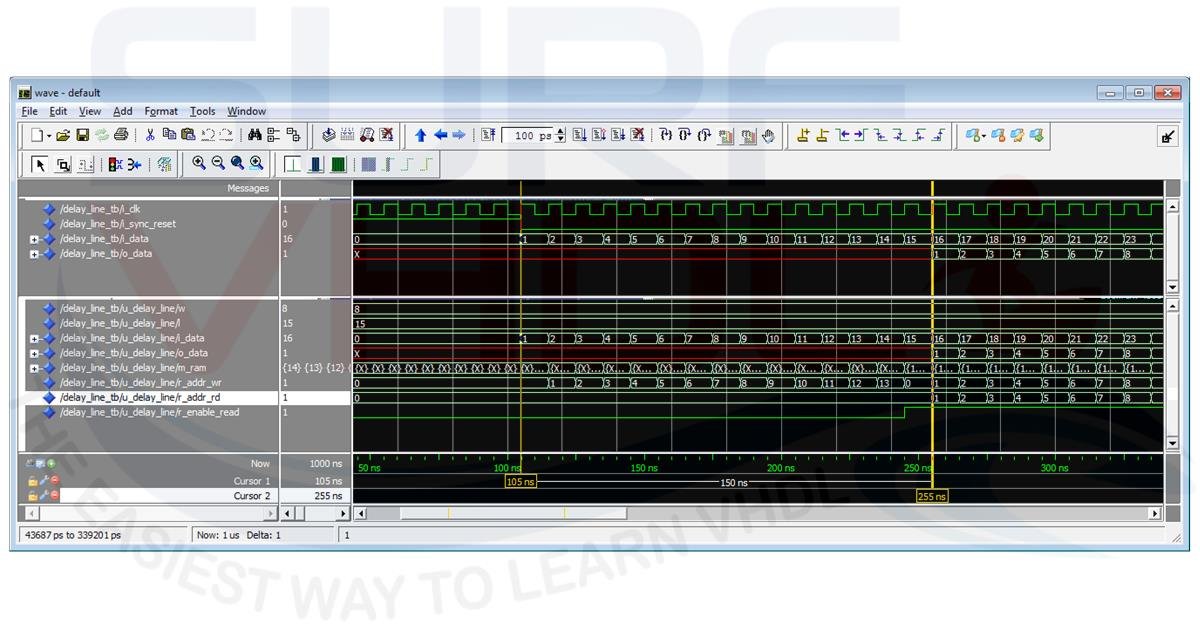
Figure5 – Modelsim simulation for VHDL code of Digital Delay Line with delay = 15
Considerations for ASIC Implementation
Pay attention if you intend to use this VHDL code for a digital delay line in ASIC technology. As you may know, ASIC technology implements dual-port RAMs as proprietary macros. Generally, you cannot infer a dual-port RAM macro directly from standard VHDL/RTL code in an ASIC flow. The solution is to instantiate the specific dual-port RAM macro as a component inside your code.
If you appreciated this post, please help us share it with your friends.
If you need to contact us, please write to: surf.vhdl@gmail.com