
Why Use a Delay Line in FPGA Design?
When you implement a digital design, one of the most used building blocks is a pipeline or a digital delay line. For instance, you could need to compensate the delay between two branches of a digital circuit in terms of clock cycles.
Figure 1 shows a possible example where you have to subtract the value of an input sample of an ADC, and this value is computed using the ADC sample itself. In the figure, the Processing Block computes the required functions over the current ADC samples. Then, the correction has to be subtracted from the current ADC input samples. Therefore, you need to compensate the processing time in terms of clock cycles using a feed-forward architecture implemented as a delay line.
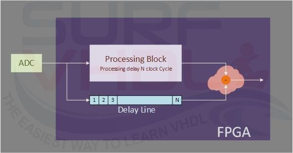
Figure 1 – An example of digital delay line requirement
The delay line can be implemented in different ways. If you use an FPGA, this device gives you different solutions, depending on how many clock cycles you need to compensate and the technology you are using:
- Shift register pipeline using flip-flops
- Shift register pipeline using block RAM or internal LUTs
- Delay line implemented using a synchronous FIFO
Shift-Register vs. FIFO: How to Choose
When deciding how to implement a delay line, the primary constraints are the delay depth (number of clock cycles) and the data width. Choosing the wrong architecture can drain logic and routing resources, increasing the fan-out and severely degrading the maximum operating frequency (Fmax). Here are the general rules of thumb for modern FPGAs:
- Short Delays (e.g., < 16-32 clock cycles): Use standard Flip-Flops (Registers). This approach is straightforward and easily meets timing without excessive routing overhead.
- Medium Delays (e.g., tens to hundreds of cycles): Rely on Shift-Register LUTs (like Xilinx SRL16/SRL32 or Altera altshift_taps) or Block RAM. Synthesis tools will automatically infer these primitives to save logic, provided you remove asynchronous resets from the data path.
- Long Delays or High Data Widths: Implement a Synchronous FIFO. Large plain shift registers consume massive resources and negatively impact Fmax. A dedicated FIFO efficiently leverages Block RAM primitives and provides a robust solution.
Use the calculator below to quickly estimate the total bits of your delay line and find the recommended FPGA implementation strategy.
Shift-Register Implementation (Flip-Flops and Block RAM)
The register pipeline has a straightforward implementation. A VHDL example of a pipeline delay line is:
library ieee;
use ieee.std_logic_1164.all;

entity shift_register_parametric is
generic(
  G_WIDTH                 : integer := 8;
  G_DEPTH                 : integer := 24);
port (
  i_clk                       : in  std_logic;
  i_rstb                      : in  std_logic;
  i_d                         : in  std_logic_vector(G_WIDTH-1 downto 0);
  o_q                         : out std_logic_vector(G_WIDTH-1 downto 0));
end shift_register_parametric;

architecture rtl of shift_register_parametric is

type t_q_pipe is array(0 to G_DEPTH-1) of std_logic_vector(G_WIDTH-1 downto 0);
signal q_pipe          : t_q_pipe;

begin

process_pipe : process(i_clk,i_rstb)
begin
  if(i_rstb='0') then
    q_pipe   <= (others=>(others=>'0'));
  elsif(rising_edge(i_clk)) then

    q_pipe   <= i_d&q_pipe(0 to q_pipe'length-2);

  end if;
end process process_pipe;

o_q <= q_pipe(q_pipe'length-1);

end rtl;
If you remove the reset signal i_rstb, the synthesizers will implement the shift register in dedicated FPGA logic resources, if available. The VHDL code for this optimized shift register implementation using internal Block RAM or LUTs is:
library ieee;
use ieee.std_logic_1164.all;

entity delay_line_parametric is
generic(
  G_WIDTH                 : integer := 8;
  G_DEPTH                 : integer := 24);
port (
  i_clk                       : in  std_logic;
  i_d                         : in  std_logic_vector(G_WIDTH-1 downto 0);
  o_q                         : out std_logic_vector(G_WIDTH-1 downto 0));
end delay_line_parametric;

architecture rtl of delay_line_parametric is

type t_q_pipe is array(0 to G_DEPTH-1) of std_logic_vector(G_WIDTH-1 downto 0);
signal q_pipe          : t_q_pipe;

begin

process_pipe : process(i_clk)
begin
  if(rising_edge(i_clk)) then

    q_pipe   <= i_d&q_pipe(0 to q_pipe'length-2);

  end if;
end process process_pipe;

o_q <= q_pipe(q_pipe'length-1);

end rtl;
In Altera Cyclone III FPGA technology, for example, the shift register is implemented as shown in Figure 2:
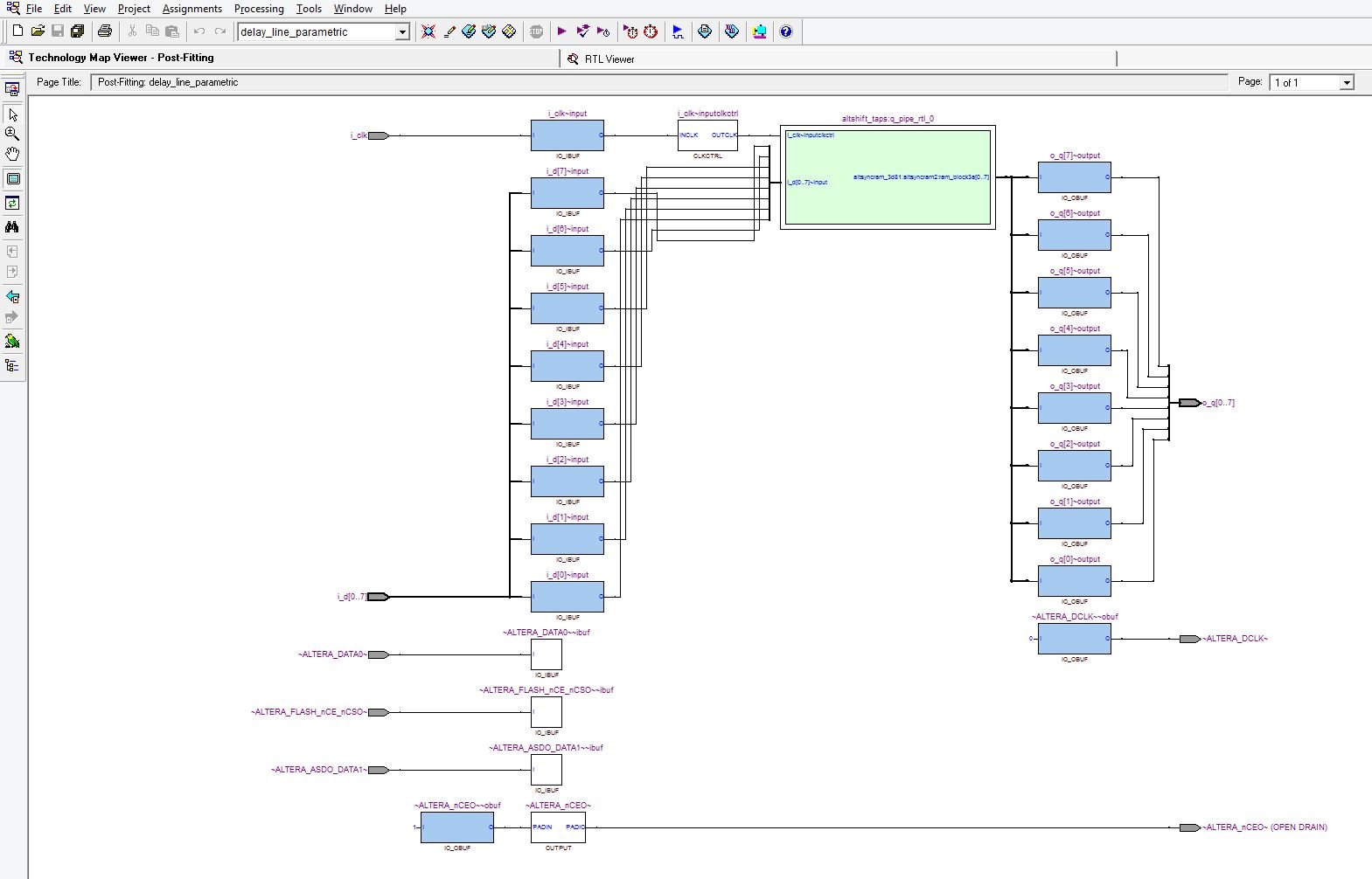
Figure 2 – Quartus II MAP Viewer for Delay Line implementation in Cyclone III FPGA
Synchronous FIFO Implementation
If the delay line is demanding in terms of the number of bits to be stored, the delay line is implemented using a synchronous FIFO memory. As explained in Figure 3, the input i_rstb signal enables writing data into the FIFO when high; when low, it resets the delay counter and the FIFO control logic. Clearly, i_rstb acts as a synchronous reset/enable of the delay line.
The input data and the reset signal are re-synchronized with the input clock to avoid problems in a synchronous design implementation. Generally, the reset signal of the synchronous FIFO macro in the FPGA is a synchronous signal.
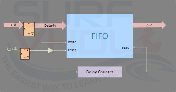
Figure 3 – FIFO Implementation of Digital Delay Line
A possible VHDL code implementation of the delay line implemented as a FIFO in FPGA is:
library ieee;
use ieee.std_logic_1164.all;

entity shift_register_fifo is
generic(
  G_WIDTH                 : integer := 8;   -- FIFO shall be compliant
  G_DEPTH                 : integer := 24); -- G_DEPTH > 3
port (
  i_clk                       : in  std_logic;
  i_rstb                      : in  std_logic;
  i_d                         : in  std_logic_vector(G_WIDTH-1 downto 0);
  o_q                         : out std_logic_vector(G_WIDTH-1 downto 0));
end shift_register_fifo;

architecture rtl of shift_register_fifo is

component alt_fifo_1kx8
port (
  aclr        : in std_logic ;
  clock       : in std_logic ;
  data        : in std_logic_vector (7 downto 0);
  rdreq       : in std_logic ;
  wrreq       : in std_logic ;
  almost_full : out std_logic ;
  empty       : out std_logic ;
  q           : out std_logic_vector (7 downto 0));
end component;

signal aclr             : std_logic ;
signal data             : std_logic_vector (7 downto 0);
signal rdreq            : std_logic ;
signal wrreq            : std_logic ;
signal delay_counter    : integer;

begin

process_control : process(i_clk)
begin
  if(rising_edge(i_clk)) then
    data            <= i_d;  -- resync data in
    if(i_rstb='0') then
      delay_counter   <= 0;
      wrreq           <= '0';
      rdreq           <= '0';
      aclr            <= '1';
    elsif(delay_counter<G_DEPTH-2) then
      delay_counter   <= delay_counter + 1;
      wrreq           <= '1';
      rdreq           <= '0';
      aclr            <= '0';
    else
      wrreq           <= '1';
      rdreq           <= '1';
      aclr            <= '0';
    end if;
  end if;
end process process_control;

u_alt_fifo_1kx8 : alt_fifo_1kx8
port map(
  aclr        => aclr        ,
  clock       => i_clk       ,
  data        => data        ,
  rdreq       => rdreq       ,
  wrreq       => wrreq       ,
  almost_full => open        ,
  empty       => open        ,
  q           => o_q         );
end rtl;
In the entity/architecture pair implementation, the FIFO width shall be matched with the input data. The FIFO depth shall be greater than the delay line length.
Simulation and Synthesis Results
The simulation wave in Figure 4 compares the three outputs of the different delay line implementations:
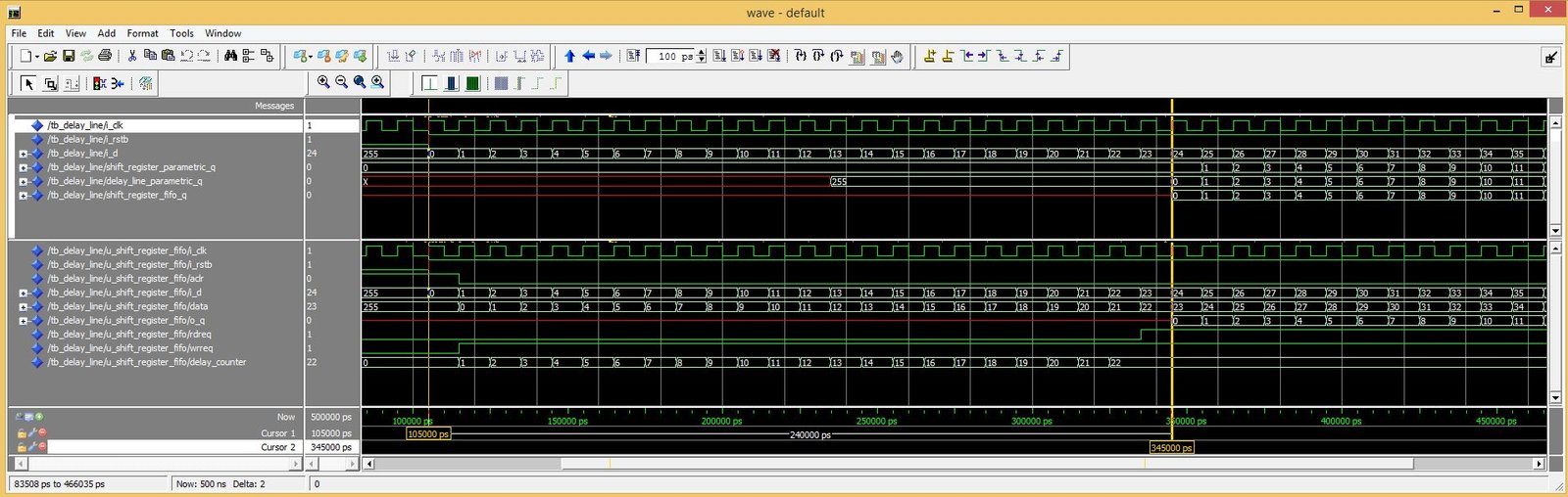
Figure 4 – Simulation result of different VHDL implementations of Shift Register
- Shift register delay line implementation
- Shift register optimized for internal FPGA block RAM implementation
- Delay line implemented using a FIFO
It is worth noting that Altera Quartus II implements both Shift register delay line architecture versions (with and without asynchronous reset) using the internal altshift_taps macro, optimizing internal flip-flop area usage.