
How to Compute the Frequency of a Clock in FPGA
When you use an FPGA, you always need a clock. However, when you start debugging your VHDL layout code on the FPGA, your design often doesn’t work as it should!
It’s the hardware, my friend!
Digital design has a big advantage compared to analog design: if you implement a good synchronous design and simulate it, you can be very confident that the design will work as intended.
But the reality is different!
I have bad news: when you start debugging your design on an FPGA, it almost never works on the first try… Did this ever happen to you?
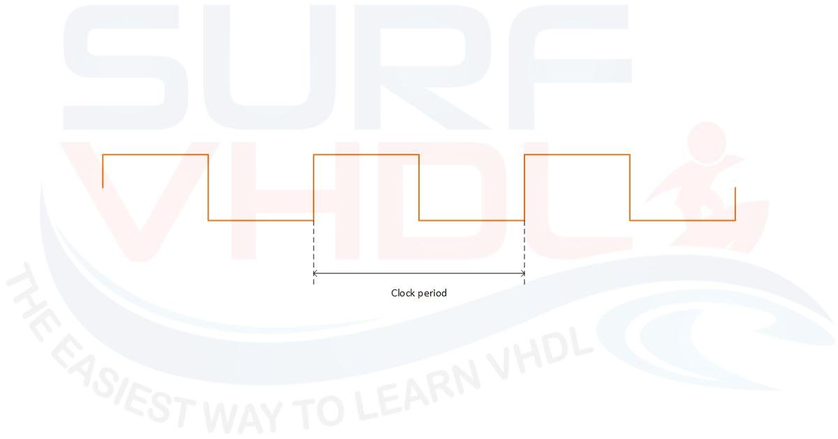
Figure1 – clock signal example
There is also good news: if you performed a thorough simulation of your digital design, the problems you encounter during board testing are typically of the same type:
- you didn’t handle the reset pin correctly
- the clock signal is absent or has an incorrect frequency
Maybe you are thinking: it is not possible that the main errors are just the clock and the reset!
Well, if you simulated your VHDL design and respected the golden rules of digital design (you can find some examples and the available courses here), external reset and clock signals are indeed the most common issues!
How to Detect an FPGA Clock Signal
For the reset pin, the solution is very simple: you can map the reset signal to an output pin connected to an LED so you can easily check if it is working fine.
What about the clock?
Here the issue is a bit different. The clock is a periodic signal changing extremely fast, so you cannot directly connect it to an LED. But… if you divide the clock rate down to a “human-readable” frequency, you can use it to blink an LED.
In other words, you can connect the clock to a module that implements a counter to generate a slow signal. This signal can drive an LED at a toggling rate of, for instance, one second. Doing this allows you to monitor if your clock is physically present.
This is a good starting solution, but… how can you actually measure the exact clock frequency? You can guess an approximate value from the blinking rate, but it remains a rough estimation.
The Theory Behind Digital Clock Frequency Measurement
If we need to verify the exact clock frequency, we can use an oscilloscope or count the clock rate digitally.
The oscilloscope solution doesn’t need a blog post, so let’s see how to implement a digital clock frequency counter inside the FPGA.
The basic architecture is reported in the figure below:
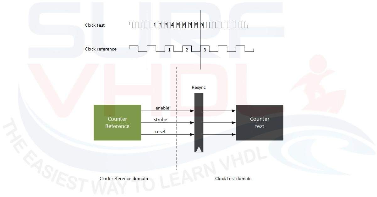
Figure2 – Clock counter architecture with CDC synchronization
As you can see, we use a known reference clock to measure an unknown test clock.
The reference clock counts up to a fixed number of clock cycles to define a precise time interval (gating window). For instance, if the reference clock is 50 MHz (period of 20 ns) and the counting limit is 2^12, the gating window is:
20 ns × 2^12 = 81920 ns = 81.92 µs
To compute the test clock frequency, we need to know how many clock cycles of the test clock occur within this reference gating interval. We use the reference clock counter to start and stop the test clock counter.
Practical Examples
Let’s clarify this with two practical examples.
Example 1: Test Clock is 125 MHz
- Reference clock: 50 MHz (20 ns)
- Reference clock count: 2^12 (4096 cycles)
During this reference interval, the test clock counter reaches 10240 cycles.
The computed test clock frequency is:
10240 / 4096 × 50 MHz = 2.5 × 50 = 125 MHz (8 ns)
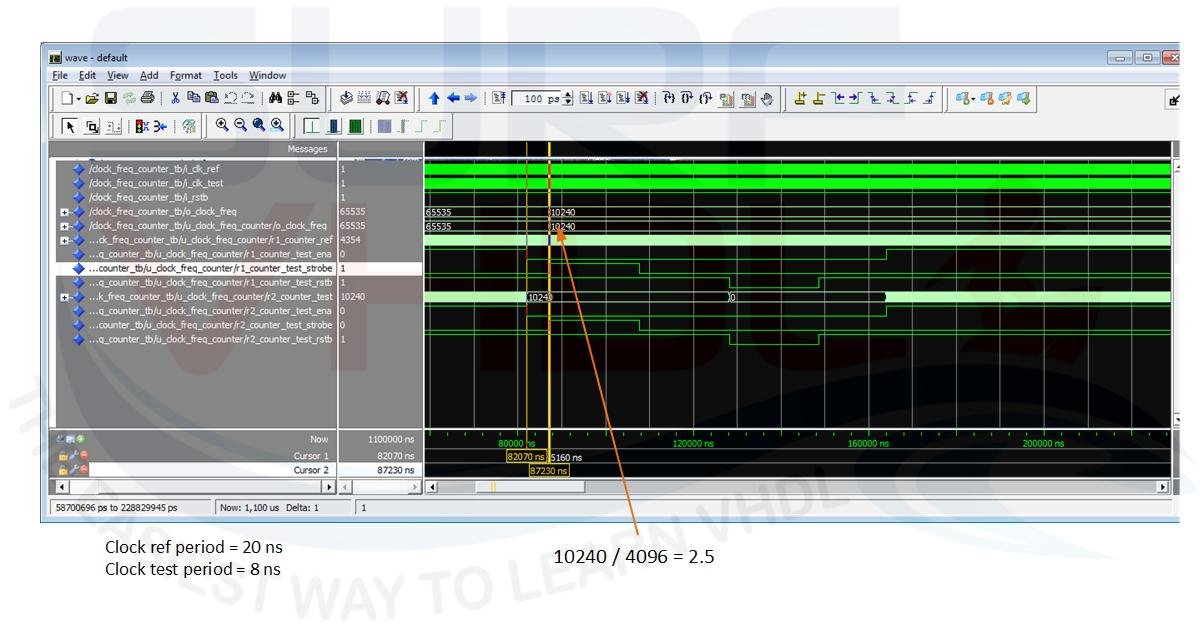
Figure3 – VHDL clock counter simulation with a 125 MHz test clock
Example 2: Test Clock is 25 MHz
If the test clock counter reaches 2048 during the same reference interval, the computed frequency is:
2048 / 4096 × 50 MHz = 0.5 × 50 = 25 MHz (40 ns)
This scenario is reported in the simulation in Figure4.
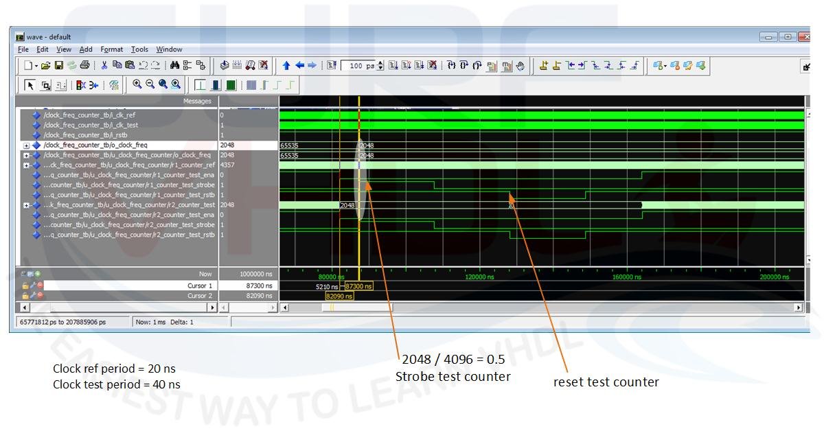
Figure4 – VHDL clock counter simulation with a 25 MHz test clock
Try It Yourself: Interactive Clock Counter Simulator
Experiment with the reference clock frequency, counter size, and test clock frequency. The simulator computes the gating window, expected count, frequency resolution, and quantization error, and draws a split-axis timing diagram showing the REF CLOCK, GATE WINDOW, CDC-synchronized enable, and TEST CLOCK signals.
FPGA Clock Counter Calculator & Simulator
Simulate visual Gating Windows, analyze Clock Domain Crossing (CDC) signals, and calculate real-time resolutions.
Input Parameters
Measurement Metrics
Split-Axis Timing Diagram (Gating Window In-Scale)
Measurement Resolution
Since the reference clock and the test clock are completely asynchronous, the starting and ending edges of the gating window do not line up with the test clock edges. This misalignment introduces a classic ±1 cycle quantization error on the test counter.
The frequency resolution corresponds to the weight of exactly one count:
frequency_resolution = freq_ref / 2^12
For our 50 MHz reference clock and 2^12 counter, the resolution is:
50 MHz / 4096 ≈ 12.2 kHz
This means that any measurement we carry carries an intrinsic uncertainty of about 12.2 kHz. If you need higher precision, you can simply increase the reference counter bits (e.g., using 2^13 or 2^14 cycles), which lengthens the gating window and reduces the measurement resolution.
VHDL Implementation
While the basic idea of clock frequency computation is very simple, we must pay close attention when implementing the actual VHDL component.
Because the reference clock and the test clock are completely asynchronous, we are crossing different asynchronous clock domains. We must carefully manage Clock Domain Crossing (CDC) to avoid timing violations and metastability.
In the VHDL code below, the control signals generated in the reference clock domain (r1_counter_test_ena, r1_counter_test_strobe, and r1_counter_test_rstb) are synchronized into the test clock domain.
In this educational VHDL implementation, we synchronize the signals using a single-stage register (p_clk_test_resync). In highly reliable production systems, crossing asynchronous domains requires a double flip-flop synchronizer (two cascaded registers clocked by i_clk_test) to reduce the probability of metastability to negligible levels. Without proper synchronization, the layout tool cannot guarantee timing closure, and the control logic in the test clock domain could behave unpredictably.
Below is the complete VHDL implementation:
library ieee;
use ieee.std_logic_1164.all;
use ieee.numeric_std.all;

entity clock_freq_counter is
    port (
        i_clk_ref    : in  std_logic;
        i_clk_test   : in  std_logic;
        i_rstb       : in  std_logic;
        o_clock_freq : out std_logic_vector(15 downto 0)
    );
end clock_freq_counter;

architecture rtl of clock_freq_counter is
    -- r1_ prefixes: registers in the reference clock domain
    -- r2_ prefixes: registers in the test clock domain

    -- REFERENCE CLOCK Domain Signals
    signal r1_counter_ref         : unsigned(12 downto 0); -- 12+1 bit: MSB is used for test counter control
    signal r1_counter_test_ena    : std_logic;
    signal r1_counter_test_strobe : std_logic;
    signal r1_counter_test_rstb   : std_logic;

    -- TEST CLOCK Domain Signals
    signal r2_counter_test        : unsigned(15 downto 0); -- Test clock can be up to 16x reference clock
    signal r2_counter_test_ena    : std_logic;
    signal r2_counter_test_strobe : std_logic;
    signal r2_counter_test_rstb   : std_logic;

begin

    -- REFERENCE CLOCK Domain Process
    p_counter_ref : process (i_rstb, i_clk_ref)
    begin
        if (i_rstb = '0') then
            r1_counter_ref         <= (others => '0');
            r1_counter_test_ena    <= '0';
            r1_counter_test_strobe <= '0';
            r1_counter_test_rstb   <= '0';
        elsif rising_edge(i_clk_ref) then
            r1_counter_ref <= r1_counter_ref + 1; -- Free running counter

            -- Use the MSB to control the test counter enable signal
            r1_counter_test_ena <= not r1_counter_ref(r1_counter_ref'high);

            -- Generate the strobe signal to store the count
            if (r1_counter_ref > 16#1100#) and (r1_counter_ref < 16#1500#) then
                r1_counter_test_strobe <= '1';
            else
                r1_counter_test_strobe <= '0';
            end if;

            -- Generate the reset signal for the test counter
            if (r1_counter_ref > 16#1900#) and (r1_counter_ref < 16#1D00#) then
                r1_counter_test_rstb <= '0';
            else
                r1_counter_test_rstb <= '1';
            end if;
        end if;
    end process p_counter_ref;

    -- Clock Domain Crossing (CDC) Resynchronization
    p_clk_test_resync : process (i_clk_test)
    begin
        if rising_edge(i_clk_test) then
            r2_counter_test_ena    <= r1_counter_test_ena;
            r2_counter_test_strobe <= r1_counter_test_strobe;
            r2_counter_test_rstb   <= r1_counter_test_rstb;
        end if;
    end process p_clk_test_resync;

    -- TEST CLOCK Domain Process
    p_counter_test : process (r2_counter_test_rstb, i_clk_test)
    begin
        if (r2_counter_test_rstb = '0') then
            r2_counter_test <= (others => '0');
        elsif rising_edge(i_clk_test) then
            if (r2_counter_test_ena = '1') then
                r2_counter_test <= r2_counter_test + 1;
            end if;
        end if;
    end process p_counter_test;

    -- Output Register Process
    p_counter_test_out : process (i_rstb, i_clk_test)
    begin
        if (i_rstb = '0') then
            o_clock_freq <= (others => '1'); -- Set all bits to '1' on reset or if test clock is absent
        elsif rising_edge(i_clk_test) then
            if (r2_counter_test_strobe = '1') then
                o_clock_freq <= std_logic_vector(r2_counter_test);
            end if;
        end if;
    end process p_counter_test_out;

end rtl;
In this VHDL code, the r1_ and r2_ prefixes represent registers belonging to the reference and test clock domains respectively. As shown, the process p_clk_test_resync handles the clock domain crossing by registering the reference domain control signals using the test clock.
Counter Wrap-around Handling
The reference counter is set to 12 bit and the test counter to 16 bit. The test clock can run up to 16 times faster than the reference clock (2^16 / 2^12 = 16). If the test clock runs faster than 16 times, the 16-bit counter will wrap around and we will detect the wrong frequency.
If we are aware of this limit, we can compensate the wrap around in the clock computation equation by adding 2^16 to the clock test counter value.
For instance, reference clock = 1 MHz, test clock = 18 MHz. Every 2^12 reference clock cycles, the test clock counter will count:
2^12 × 18 = 73728
but if we are using a 16 bit counter the value we get will be:
73728 − 65536 = 8192
In this case, if we do not take into account the counter wrapping, the frequency we compute will be:
8192 / 2^12 × 1 MHz = 0.5 MHz
instead of 18 MHz!
How Slow Can the Test Clock Be?
In this implementation, the strobe signal is stable for 256 reference clock cycles, then the reset signal is asserted 1024 reference clock cycles after the strobe signal de-asserts. Using this strategy, the clock frequency counter can also work with a test clock up to 256 times slower than the reference clock.
In the simulations of Figure3 and Figure4 there are examples with test clock faster than reference and test clock slower than reference.
Clock Counter VHDL Code Live Demo
In the video below you can watch a live demo of this clock frequency counter implementation.
The design is implemented on a Terasic Altera DE0 board. We use an internal PLL to generate different internal clocks, which are selected using physical DIP switches (as illustrated in Figure5).
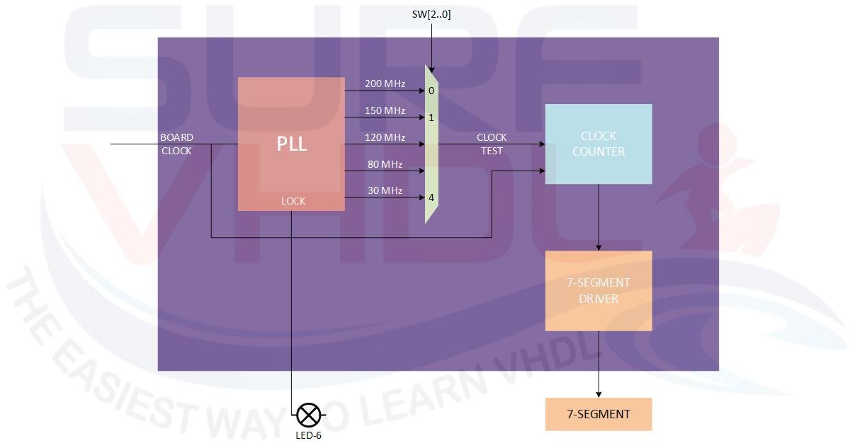
Figure5 – Clock counter test architecture on a DE0 board
The selected clock acts as the test clock, while the 50 MHz onboard clock serves as the reference clock. The estimated clock frequency is displayed on the onboard 7-segment display in hexadecimal format.
The clock frequency can be estimated as:
HEX_VALUE / 2^12 × 50 MHz
Click Here to enroll the free course
“How To Measure Clock Frequency in FPGA”
If you appreciated this post, please help us to share it with your friends.
If you need to contact us, please write to: surf.vhdl@gmail.com