Basic notion on FIFO (First-In First-Out)
FIFO means First-In First-Out. A FIFO is a structure used in hardware or software application when you need to buffer a data.
Basically, you can think about a FIFO as a bus queue in London.
The people that arrive first is the one who catch the bus first….

Of course, this example is valid only in London or in Japan, in other countries, it could be not be used 🙂
How can you implement a FIFO structure?
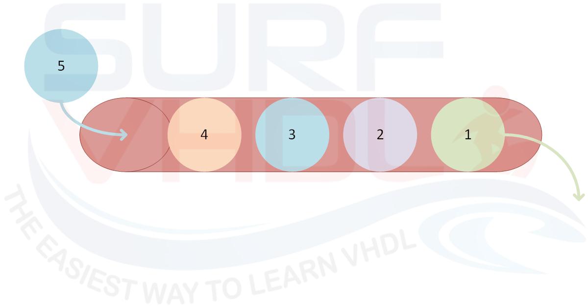
As a basic idea, you can imagine a FIFO as a pipe where the first element entering into the pipe is the first element that output from the pipe as clear in Figure2.
In particular, you can implement FIFO structure using a memory buffer able to store your element, plus a write pointer and read pointer in order to write data to the current memory address and read data from the memory address.
The maximum number of elements that you can store inside that memory is the FIFO depth.
The FIFO Architecture
The FIFO architecture implementation both hardware (VHDL or Verilog) or software is very similar. Of course in the hardware implementation of a FIFO, you must take into account some additional issue not present in software implementation that we will see going ahead.
In this post, we want to address first the basic architecture of a FIFO that is common either in software (C++, C#) or in hardware (VHDL, Verilog) implementation.
In Figure3, it is represented a memory that can store up to 8 elements, the memory address range is 0 to 7. The two pointer wr_ptr and rd_ptr are the write and the read pointer address respectively.
At the start, write and read pointer are set to address zero (Figure3 – A). The difference between the two pointers is zero, i.e.
wr_ptr-rd_ptr = 0
this means that the FIFO is empty.
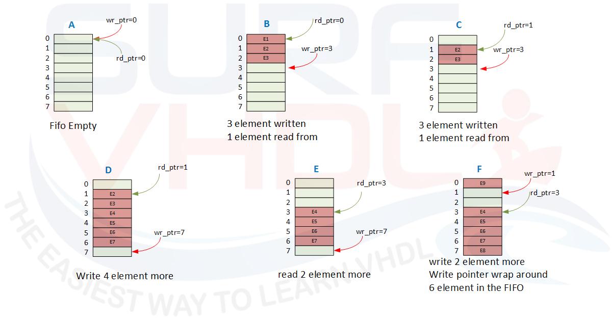
Now let write 3 elements on the FIFO (Figure3 – B):
wr_ptr = 3, point to the next valid location
rd_prt = 0

wr_ptr-rd_ptr = 3-0 = 3
the number of the elements is 3,
if we read an element from the FIFO zero memory address (Figure3 – C), Elem1 is read from FIFO and
rd_prt = 1;
in this case, the number of elements into the FIFO is
3-1 = 2
now fill the FIFO up to the 6 elements as in zero (Figure3 – D):
wr_ptr=7
rd_ptr=1

wr_ptr-rd_ptr = 7-1 = 6
read other 2 elements (Figure – E)
wr_ptr-rd_ptr = 7-3 = 4
what happen if we write another 2 elements?
current wr_ptr = 7 adding 2 elements will be 7+2=9 that is greater than FIFO depth!
Of course, we need to manage the memory as circular buffer, so the write pointer will be (Figure3 – F):
(7+2) % 8 = 1
in this case, how many data are available in the FIFO?
wr_ptr-rd_ptr = 1-3 = -2
what’s up we have -2 data??
As we stated the memory is circular buffer so the correct expression is:
(wr_ptr - rd_ptr + FIFO_DEPTH) % FIFO_DEPTH = (1-3+8)%8 = (6) % 8 = 6
if you count the number of the elements inside the FIFO is 6.
Let’s summarize, the number of data into a FIFO of depth FIFO_DEPTH is
N = (wr_ptr - rd_ptr + FIFO_DEPTH) % FIFO_DEPTH
When
N<FIFO_DEPTH and N>0 FIFO contains data
Note N in the equation above is 0 (zero) both when FIFO is empty and when FIFO is full.
So how can we detect EMPTY or FULL condition?
We have to check if write pointer is going to the read pointer or vice versa:
- if write pointer is going to the read pointer => N=0 means FIFO FULL
- if read pointer is going to the write pointer => N=0 means FIFO EMPTY
This is the basic architecture you have to know in order to understand how FIFO works.
In the software implementation, the FIFO can be implemented of custom depth without particular constraint.
Here you can find a FIFO definition and its Software implementation on Wikipedia.
FIFO Hardware Implementation Consideration
When you have to implement a FIFO in FPGA or ASIC, some consideration should be taken into account in order to simplify the FIFO realization.
FIFO depth
FIFO depth should be equal to a power of two.
As we have seen above the number of data into a FIFO is
N = (wr_ptr - rd_ptr + FIFO_DEPTH) % FIFO_DEPTH
The operation of modulo in hardware is very demanding in terms of logic gates unless FIFO_DEPTH = 2^N in this case you don’t need any check.
Maybe an example should clarify.
In the FIFO above the FIFO_DEPTH = 8 i.e. the address pointer can get the values from 0 to 7. In order to represent the address value, only 3 bits are needed.
If you need further details on the binary representation of a number you can read this post.
Let see what happen in the case of
(wr_ptr - rd_ptr + FIFO_DEPTH) % FIFO_DEPTH = (1-3+8)%8 = (6) % 8 = 6
representing wr_ptr and rd_ptr using three bits:
wr_ptr = "001" (+1d)
rd_ptr = "101" (-3d)

wr_ptr - rd_ptr =
"001" (+1) +
"101" (-3) =
-----------------
"110" = 6
the modulo operation is self-contained into 2’complement arithmetic.
So as a rule of thumb if you use power of two for FIFO_DEPTH the number of data into a circular buffer is simply given by
(wr_ptr – rd_ptr)
represented with log2(FIFO_DEPTH) number of bits.
in the example above
2^3 = 8
How to implement a FIFO into FPGA?
Until now we have considered the general FIFO architecture:
- memory element
- write pointer
- read pointer
- the relationship between write and read pointer.
When you deal with FPGA or ASIC hardware implementation the going get tough!
Typical FIFO FPGA or ASIC hardware architecture (Figure4 ) is implemented using a
- DUAL-PORT RAM
- write counter to address the write side of the RAM
- read counter to address the write side of the RAM
- control logic aiming to update the write counter, at each write data into the RAM, and the read counter, every time a data is read from RAM.
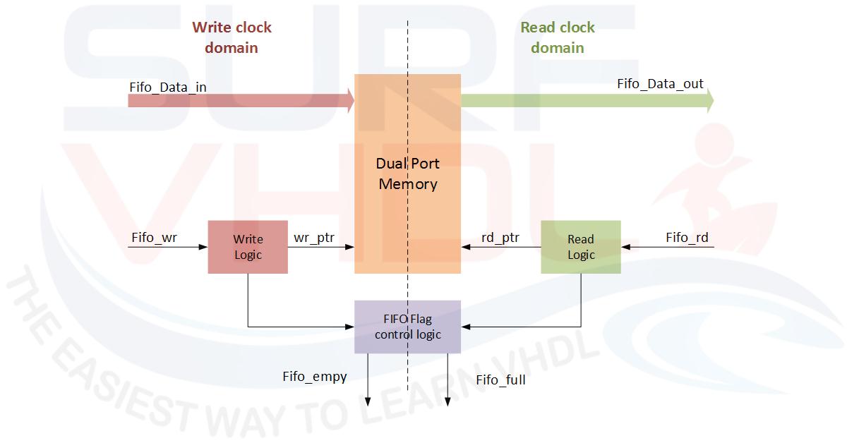
Moreover, the control logic shall drive the FIFO flag
- FIFO-Empty: flags no data is present inside the FIFO RAM
- FIFO-Full: no data can be written to FIFO memory
- FIFO-Almost Empty/Full: if required
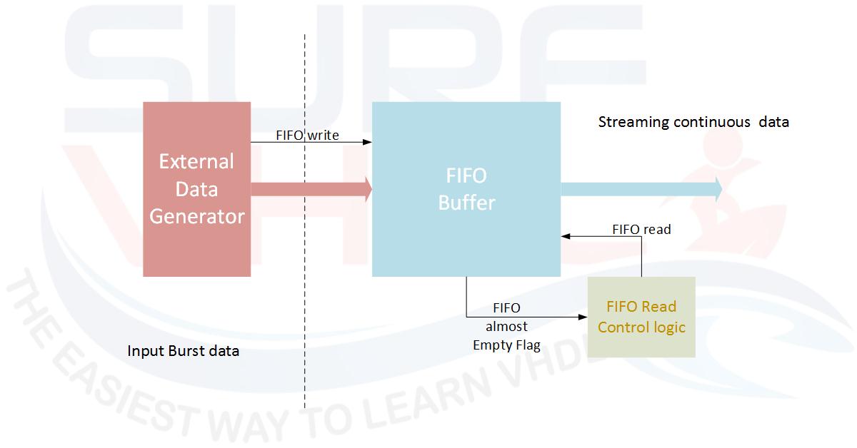
A typical use of the FIFO-Almost Empty flags is when the FIFO is used in order to buffer input data stream of a device where the input and output data throughput is the same but the timing is different as in Figure5:
- Input as burst data;
- Output as continuous data.
- The FIFO is used to buffer the minimum number of burst data in order to guarantee continuous reading from FIFO without interruption.
In this case, the FIFO Read Control Logic block check for almost empty flag going high and set FIFO read control signal to read continuously from FIFO.
A typical use of the FIFO-Almost Full flag is a module connected to an output FIFO generating streaming data at a higher rate with respect to the output and the almost full flag is used to block data generation as in Figure6.
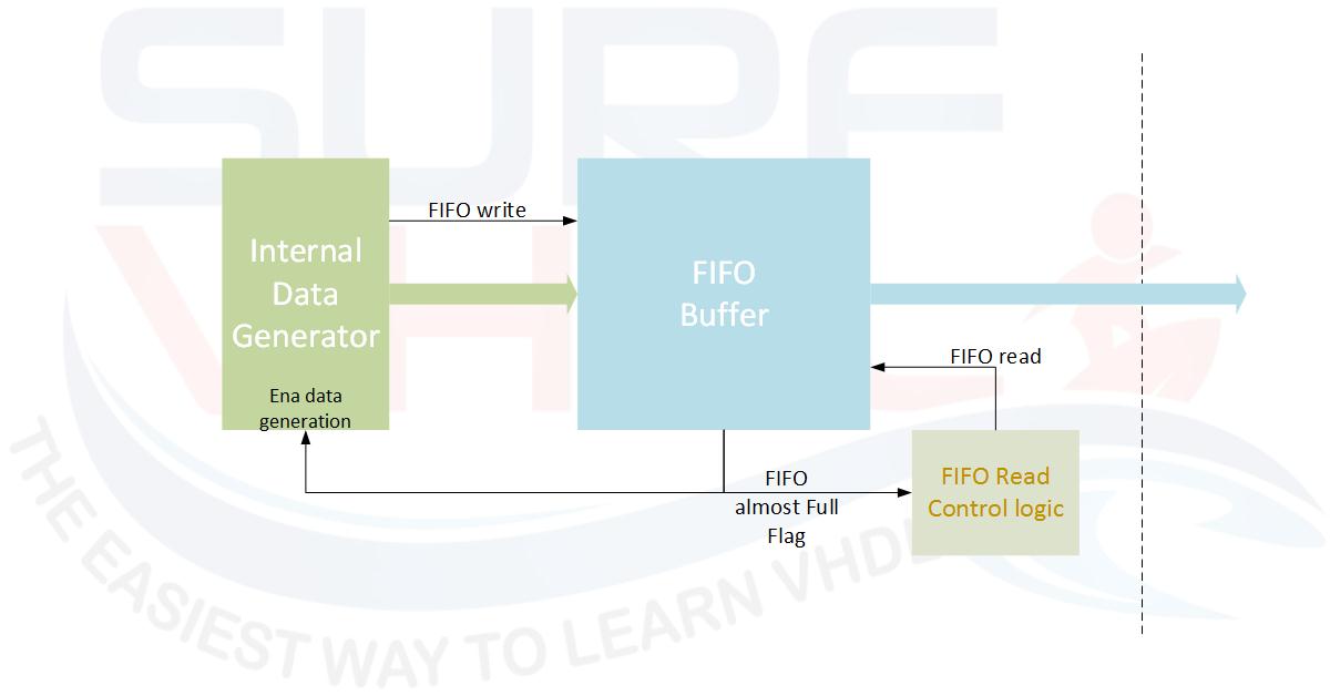
Even in this case, the FIFO Read Control Logic block check for almost full flag going high and set FIFO read control signal to read continuously from FIFO. The same almost full flag is used to stop data generation from the Internal Data Generator module. The overall results is that the data written into the FIFO is generated as burst, at the FIFO output the data is streamed continuously.
FIFO last consideration
In both cases above, the FPGA or ASIC hardware implementation of the FIFO can implement two potential different clock domains. If different clock domains are required, the FIFO shall be designed as asynchronous FIFO.
The FIFO implementation became more complex if the write side and read side of the FIFO are driven by different clock domains.
The write clock domain side will update the write pointer address and write data on the half memory clocked by the write clock.
The read clock domain side will update the read pointer address and read data from the half memory clocked by the read clock.
In this case, particular attention shall be taken into account during the EMPTY/FULL flag updating: the FIFO flags are updated crossing the two clock domain. There are several techniques used to implement Clock Cross Domain. In FPGA or ASIC the most used strategy is to gray codify the write and read counter. In this case, the pointer can set only one bit per increment, switching the minimum number of bits during the update. This counter update strategy minimizes the error during the cross check write/read at two different clocks.
Generally, you should not write a VHDL of Verilog code for a FIFO but you should use the vendor macro that guarantees you the correct FIFO functionality both on synchronous and asynchronous write and read clock, i.e. using or not the same clock in write and read side.
Here you can find an example of FIFO implementation in Altera technology;
Here you can find an example of FIFO implementation in Xilinx technology;
If you appreciated this post, please help us to share it with your friend.
[social_sharing style=”style-7″ fb_like_url=”https://surf-vhdl.com/what-is-a-fifo” fb_color=”light” fb_lang=”en_US” fb_text=”like” fb_button_text=”Share” tw_lang=”en” tw_url=”https://surf-vhdl.com/what-is-a-fifo” tw_button_text=”Share” g_url=”https://surf-vhdl.com/what-is-a-fifo” g_lang=”en-GB” g_button_text=”Share” linkedin_url=”https://surf-vhdl.com/what-is-a-fifo” linkedin_lang=”en_US” alignment=”center”]
If you need to contact us, please write to: surf.vhdl@gmail.com
We appreciate any of your comment, please post below:
Thanks!
You are welcome!
Beneficial 🙂
Thank You!
i really appreciate your efforts in writing this blog. The information provided is very easily understandable. Thanks for making efforts.
thank you very much for your feedback!
Really thankful for your kindness 🙏
you are welcome!
How the strings IDLE, WRITE, READ are written in the output waveform? What is the command used to display the string?
need some more detailed how FIFO is working
very nice
How did you consider 101 as -3 ? Can’t it be 5?
depend if your representation is signed or unsigned.
If signed, and you have only 3 bits, the value is 5-2^3=-3