How To Implement Shift-Register in VHDL Using a FIFO
When you implement a digital design one of the most used building block is a pipeline or a digital delay line. For instance, you could need to compensate the delay between two
For instance, you could need to compensate the delay between two branches of a digital circuit in terms of clock cycle. In
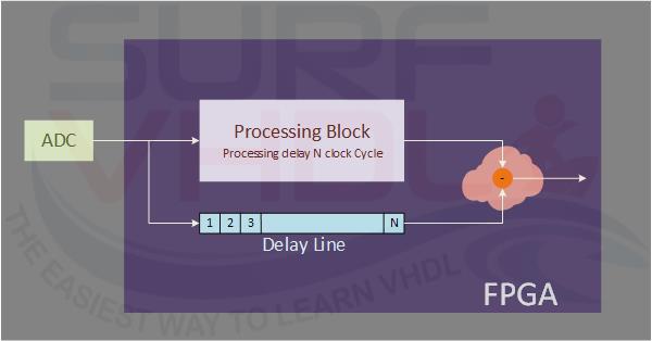
In Figure1, there is a possible example where you have to subtract the value of an input sample of an ADC and this value is computed using the ADC sample as well. In the figure, the “Processing Block” compute the required functions over the current ADC samples. Then the correction has to be subtracted to the current ADC input samples. So you need to compensate the processing time in terms of clock cycle using a feed-forward architecture implemented as a delay line.
The delay line can be implemented in different ways. If you use an FPGA, this device gives you different solutions, depending on how many clock cycles you need to compensate and the device you are using:
- Shift register pipeline as flip-flop
- Shift register pipeline as block RAM or internal LUT depending on technology
- Delay line implemented as FIFO
Shift-Register Implementation of Digital Delay Line
The register pipeline has a straightforward implementation. A VHDL example of pipeline delay line can be:
library ieee;
use ieee.std_logic_1164.all;

entity shift_register_parametric is
generic(
  G_WIDTH                 : integer := 8;
  G_DEPTH                 : integer := 24);
port (
  i_clk                       : in  std_logic;
  i_rstb                      : in  std_logic;
  i_d                         : in  std_logic_vector(G_WIDTH-1 downto 0);
  o_q                         : out std_logic_vector(G_WIDTH-1 downto 0));
end shift_register_parametric;

architecture rtl of shift_register_parametric is

type t_q_pipe is array(0 to G_DEPTH-1) of std_logic_vector(G_WIDTH-1 downto 0);
signal q_pipe          : t_q_pipe;

begin

process_pipe : process(i_clk,i_rstb)
begin
  if(i_rstb='0') then
    q_pipe   <= (others=>(others=>'0'));
  elsif(rising_edge(i_clk)) then

    q_pipe   <= i_d&q_pipe(0 to q_pipe'length-2);

  end if;
end process process_pipe;

o_q <= q_pipe(q_pipe'length-1);

end rtl;
If you remove the reset signal “i_rstb” the synthesizers will implement the shift-register in a dedicated FPGA logic resources, if available. The VHDL code for this optimized shift register implementation using internal Block RAM or LUT can be:
library ieee;
use ieee.std_logic_1164.all;

entity delay_line_parametric is
generic(
  G_WIDTH                 : integer := 8;
  G_DEPTH                 : integer := 24);
port (
  i_clk                       : in  std_logic;
  i_d                         : in  std_logic_vector(G_WIDTH-1 downto 0);
  o_q                         : out std_logic_vector(G_WIDTH-1 downto 0));
end delay_line_parametric;

architecture rtl of delay_line_parametric is

type t_q_pipe is array(0 to G_DEPTH-1) of std_logic_vector(G_WIDTH-1 downto 0);
signal q_pipe          : t_q_pipe;

begin

process_pipe : process(i_clk)
begin
  if(rising_edge(i_clk)) then

    q_pipe   <= i_d&q_pipe(0 to q_pipe'length-2);

  end if;
end process process_pipe;

o_q <= q_pipe(q_pipe'length-1);

end rtl;
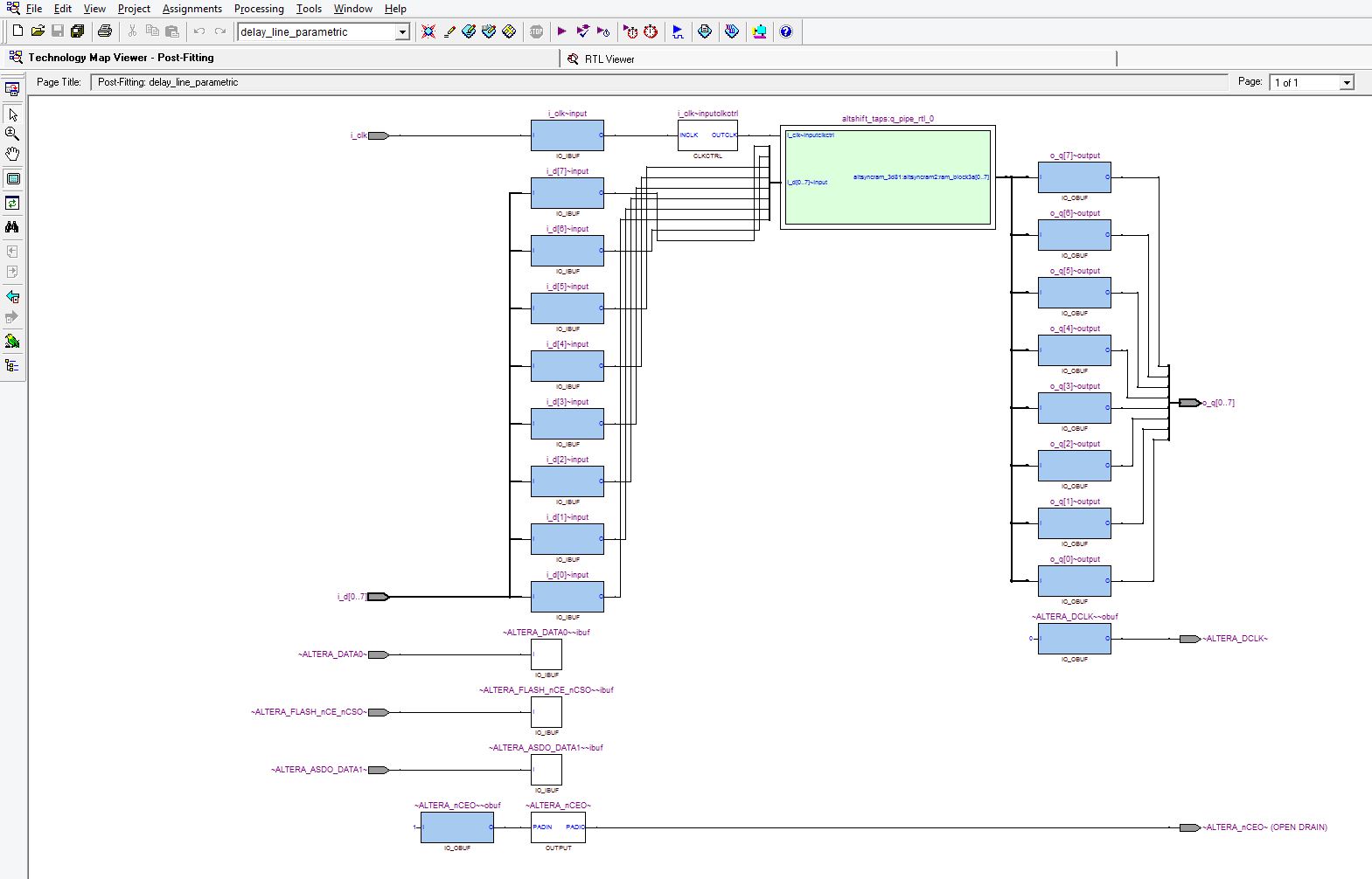
In Altera Cyclone III FPGA technology, for example, shift register is implemented as Figure2:
If the delay line is demanding in terms of a number of bits to be stored, the FIFO implementation could be a very efficient solution.
FIFO Implementation of Digital Delay Line
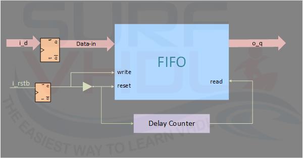
In this case, the delay line is implemented using the synchronous FIFO memory. As explained in Figure3, in this case the input “i_rstb” signal is used to enable write data into the FIFO when high, when low reset the delay counter and the FIFO control logic. As clear the “i_rstb” is used as synchronous reset/enable of the delay line. This is an efficient approach when a long delay line is requested.
This is an efficient approach when a long delay line is requested.
The input data and the reset signal are re-synchronized with the input clock to avoid the problem in synchronous design implementation. Generally, the reset signal of the synchronous FIFO macro of the FPGA is a synchronous signal.
A possible VHDL code implementation of the delay line implemented as FIFO in FPGA could be:
library ieee;
use ieee.std_logic_1164.all;

entity shift_register_fifo is
generic(
  G_WIDTH                 : integer := 8;   -- FIFO shall be compliant
  G_DEPTH                 : integer := 24); -- G_DEPTH > 3
port (
  i_clk                       : in  std_logic;
  i_rstb                      : in  std_logic;
  i_d                         : in  std_logic_vector(G_WIDTH-1 downto 0);
  o_q                         : out std_logic_vector(G_WIDTH-1 downto 0));
end shift_register_fifo;

architecture rtl of shift_register_fifo is

component alt_fifo_1kx8
port (
  aclr        : in std_logic ;
  clock       : in std_logic ;
  data        : in std_logic_vector (7 downto 0);
  rdreq       : in std_logic ;
  wrreq       : in std_logic ;
  almost_full : out std_logic ;
  empty       : out std_logic ;
  q           : out std_logic_vector (7 downto 0));
end component;

signal aclr             : std_logic ;
signal data             : std_logic_vector (7 downto 0);
signal rdreq            : std_logic ;
signal wrreq            : std_logic ;
signal delay_counter    : integer;

begin

process_control : process(i_clk)
begin
  if(rising_edge(i_clk)) then
    data            <= i_d;  -- resync data in
    if(i_rstb='0') then
      delay_counter   <= 0;
      wrreq           <= '0';
      rdreq           <= '0';
      aclr            <= '1';
    elsif(delay_counter<G_DEPTH-2) then
      delay_counter   <= delay_counter + 1;
      wrreq           <= '1';
      rdreq           <= '0';
      aclr            <= '0';
    else
      wrreq           <= '1';
      rdreq           <= '1';
      aclr            <= '0';
    end if;
  end if;
end process process_control;

u_alt_fifo_1kx8 : alt_fifo_1kx8
port map(
  aclr        => aclr        ,
  clock       => i_clk       ,
  data        => data        ,
  rdreq       => rdreq       ,
  wrreq       => wrreq       ,
  almost_full => open        ,
  empty       => open        ,
  q           => o_q         );
end rtl;
In the entity/architecture pair implementation the FIFO width shall be matched width the input data. The FIFO depth shall be greater than the delay line length.
If the number of clock cycle delay is “small” the flip-flop delay line approach should be used.
Simulation result of Digital Delay Line VHDL Implementation
The simulation wave of Figure4 compares the three outputs of the different delay line implementation:
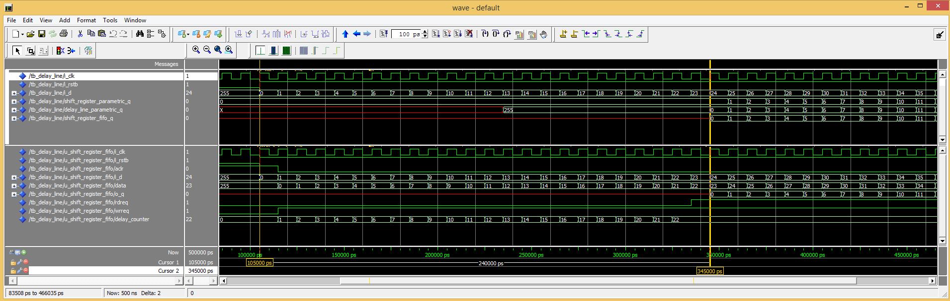
- Shift register delay line implementation;
- Shift register optimized for internal FPGA block RAM implementation
- Delay line implemented using FIFO.
It is worth of notice that Altera Quartus II implements the both Shift register delay line architecture versions (with and without asynchronous reset) using the internal “altshift_taps” macro optimizing the internal flip-flop area usage.
If you appreciated this post, please help us to share it with your friend.
[social_sharing style=”style-7″ fb_like_url=”https://surf-vhdl.com/how-to-implement-shift-register-in-vhdl-using-a-fifo” fb_color=”light” fb_lang=”en_US” fb_text=”like” fb_button_text=”Share” tw_lang=”en” tw_url=”https://surf-vhdl.com/how-to-implement-shift-register-in-vhdl-using-a-fifo” tw_button_text=”Share” g_url=”https://surf-vhdl.com/how-to-implement-shift-register-in-vhdl-using-a-fifo” g_lang=”en-GB” g_button_text=”Share” linkedin_url=”https://surf-vhdl.com/how-to-implement-shift-register-in-vhdl-using-a-fifo” linkedin_lang=”en_US” alignment=”center”]
If you need to contact us, please write to: surf.vhdl@gmail.com
We appreciate any of your comment, please post below:
Can you just help me get the “alt_fifo_1kx8” file? I am using Xilinx software. Thank you!
you need to generate it using the core generator
You can code one yourself. Just make a synchronous RAM from an array of slv and and a simple controller for read/write and some logic for the flags: full, almost_full, empty, almost_empty .
The sync RAM is sync Wr/async Rd and is simple dual port (separate Rd and Wr addr)
USE ieee.numeric_std.ALL;
USE ieee.numeric_std_unsigned.ALL;
entity alt_fifo_1kx8 is
port(
clock : in std_logic;
aclr : in std_logic;
data : in std_logic_vector(7 downto 0);
rdreq : in std_logic;
wrreq : in std_logic;
almost_full : out std_logic;
empty : out std_logic;
q : out std_logic_vector(7 downto 0)
);
end alt_fifo_1kx8;
architecture Behav of alt_fifo_1kx8 is
— 2^10 = 1024 ~ 1K… make addr 10 bits wide
constant ADDR_WIDTH : positive:= 10; — positive is subtype of intas is natural {0,1…N}, positive (1,2…N}
constant FULL_THLD : std_logic_vector(ADDR_WIDTH-1 downto 0) := (others => ‘1’); — Full thresh
constant AFULL_THLD : std_logic_vector(ADDR_WIDTH-1 downto 0) := FULL_THLD-1; — Almost Full thresh
signal Rd_addr : std_logic_vector(ADDR_WIDTH-1 downto 0):= (others => ‘0’);
signal Wr_addr : std_logic_vector(ADDR_WIDTH-1 downto 0):= (others => ‘0’);
signal Wr_en : std_logic:= ‘0’;
signal Rd_en : std_logic:= ‘0’;
signal FIFO_full : std_logic:= ‘0’;
signal FIFO_empty : std_logic:= ‘0’;
signal fbit_comp, overflow_set, underflow_set: std_logic:=’0′;
signal Addr_eq : std_logic:=’0′;
signal Addr_diff : std_logic_vector(ADDR_WIDTH-1 downto 0):=(others => ‘0’);
type mem_array is array (0 to (2**ADDR_WIDTH)-1) of std_logic_vector(7 downto 0);
signal RAM: mem_array;
begin
RAM_P: process(clock)
begin
if(rising_edge(clock)) then
if(wr_en=’1′) then
RAM(to_integer(unsigned(Wr_addr(9 downto 0)))) <= data;
end if;
end if;
end process RAM_P;
q <= RAM(to_integer(unsigned(Rd_addr(9 downto 0))));
Rd_en <= rdreq AND NOT(FIFO_empty); — can't rd from an empty FIFO
process(clock,aclr)
begin
if(aclr ='1') then
Rd_addr ‘0’);
if(rising_edge(clock)) then
if(Rd_en=’1′) then
Rd_addr <= Rd_addr + 1; — numeric_std_unsigned allows + 1 incr
end if;
end if;
end if;
end process;
Wr_en <= (not fifo_full) and wrreq; — can't write to a full FIFO
process(clock,aclr)
begin
if(aclr ='1') then
Wr_addr ‘0’);
if(rising_edge(clock)) then
if(Rd_en=’1′) then
Wr_addr <= Wr_addr + 1; — numeric_std_unsigned allows + 1 incr
end if;
end if;
end if;
end process;
— status logic
fbit_comp <= Wr_addr(ADDR_WIDTH-1) xor Rd_addr(ADDR_WIDTH-1); — XOR MSBs of Rd & Wr addresses
Addr_diff = Rd_addr
Addr_eq <= '1' when (Wr_addr = Rd_addr) else '0';
FIFO_full <= '1' when Wr_addr = FULL_THLD else '0';
empty <= (not fbit_comp) and Addr_eq;
almost_full = AFULL_THLD) else ‘0’;
empty <= FIFO_empty;
so the delay_counter will be constantly getting larger??xmmmmmm
what do you mean?