Single-port and Dual-port RAM understanding
The internal FPGA memory macro usually implements a single-port or dual-port memory as in Figure 1.
In dual-port memory implementation, we should make the distinction between simple dual-port and true dual-port RAM. In a single-port RAM, the read and write operations share the same address at port A, and the data is read from output port A. In simple dual-port RAM mode, a dedicated address port is available for each read and write operation (one read port and one write port). A write operation uses write address from port A while read operation uses read address and output from port B. In true dual-port RAM mode, two address ports are available for reading or writing operation (two read/write ports). In this mode, you can write to or read from the address of port A or port B, and the data read is shown at the output port with respect to the read address port.
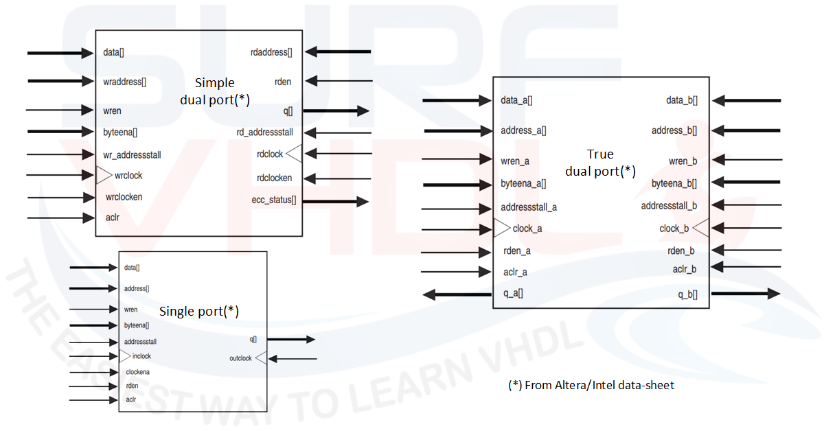
Similar consideration can be done for ROM implementation. In this case, by definition, no write port is present so the distinction is between single-port and dual-port ROM.
For instance, the dual-port ROM are generally used when we need to implement a sine/cosine table: the ROM contains the sine samples but we can address the ROM memory in order to have the sine and cosine samples ready at the output ROM port at the same time.
Implementing multi-port memory hardware architecture
Sometimes we need to write a single RAM location but to read from multiple locations at the same time. Since the FPGA technology provides a dual port memory if we need to read from, for instance, 3 different locations at the same time we have a problem. How can we solve this problem? There is no way to get into the FPGA RAM macro, so we need to implement a hardware architecture that emulates a multi-port memory. The multi-port architecture can be implemented as full VHDL/RTL code or a mixed VHDL and FPGA RAM block instance. We need to implement a hardware structure that writes simultaneously at the same RAM address and read from different RAM address in the same clock cycle. An example of multi-port memory is given in Figure 2
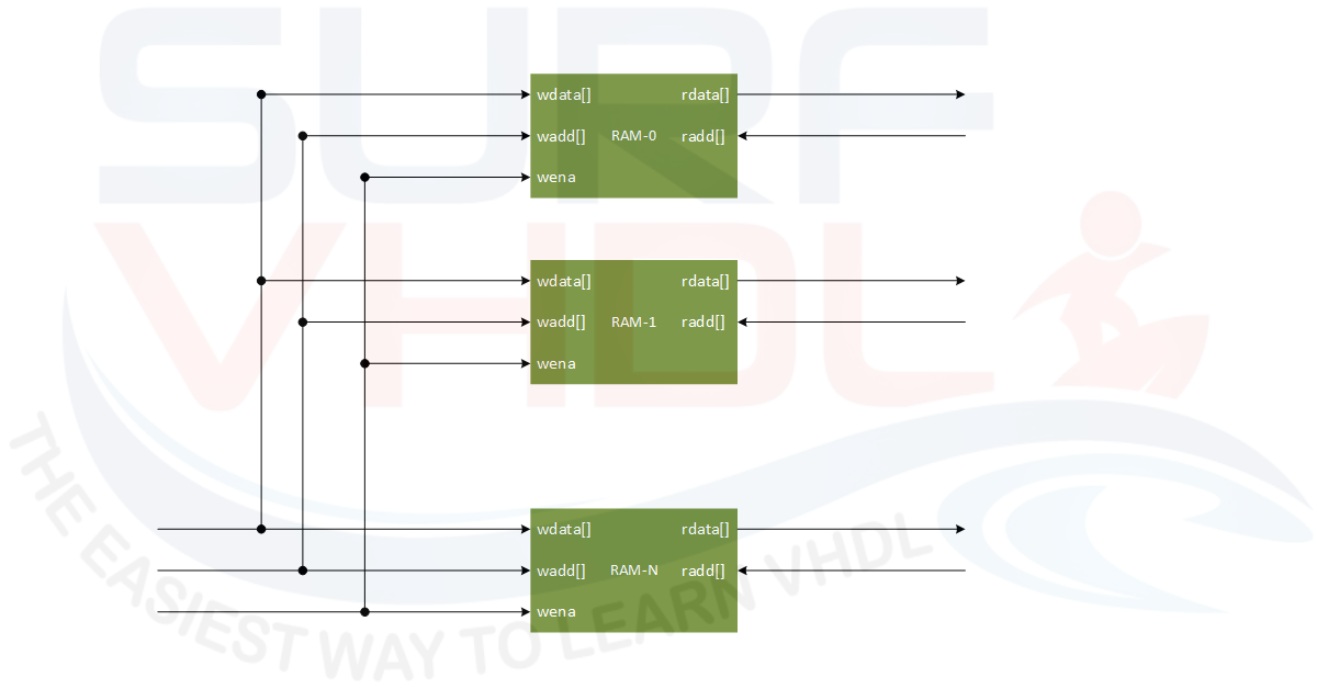
In Figure 2, the RAM blocks are implemented as simple dual-port memory:
- One write address port
- One write data port
- One read address port
- One read data port
The RAM block can be implemented either as VHDL/RTL code or using the core generator of the FPGA.
VHDL code of multi-port memory
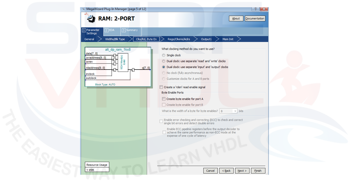
In the box below it is reported a possible implementation of multi-port RAM. In the VHDL code, the RAM block is implemented as simple dual port RAM with different write and read clock. If you don’t need different clock domains between read and write port you can connect the same clock in either write and read port. This code can be used as a template for multi-port RAM memory. The only customization you have to implement is to write the wrapper “dp_ram_simple” introducing the RAM block of your device. For instance, if you are using Xilinx technology you should use Xilinx core generator. In the case of Altera technology, you should use MegaWizard Plug-Ins in Quartus II software.
library IEEE;
use IEEE.std_logic_1164.all;
use IEEE.numeric_std.all;

entity multi_port_ram_1kx8 is
port (
  i_clk          : in  std_logic;
  i_rstb         : in  std_logic;
  -- write port
  i_wdata        : in  std_logic_vector( 7 downto 0);
  i_waddr        : in  std_logic_vector( 9 downto 0);
  i_wena         : in  std_logic;
  -- read port
  o_rdata0       : out std_logic_vector( 7 downto 0);
  o_rdata1       : out std_logic_vector( 7 downto 0);
  o_rdata2       : out std_logic_vector( 7 downto 0);
  i_raddr0       : in  std_logic_vector( 9 downto 0);
  i_raddr1       : in  std_logic_vector( 9 downto 0);
  i_raddr2       : in  std_logic_vector( 9 downto 0));
end multi_port_ram_1kx8;

architecture rtl of multi_port_ram_1kx8 is
constant C_NUM_PORT   : integer := 3;

type t_raddr is array(0 to C_NUM_PORT-1) of std_logic_vector( 9 downto 0);
type t_rdata is array(0 to C_NUM_PORT-1) of std_logic_vector( 7 downto 0);

signal w_raddr          : t_raddr;
signal w_rdata          : t_rdata;

component dp_ram_1kx8
port(
  i_rclk         : in  std_logic;
  i_wclk         : in  std_logic;
  i_rstb         : in  std_logic;
  -- write port
  i_wdata        : in  std_logic_vector( 7 downto 0);
  i_waddr        : in  std_logic_vector( 9 downto 0);
  i_wena         : in  std_logic;
  -- read port
  o_rdata        : out std_logic_vector( 7 downto 0);
  i_raddr        : in  std_logic_vector( 9 downto 0));
end component;

begin

g_multi_port_ram: for i in 0 to C_NUM_PORT-1 generate
  u_dp_ram_1kx8 : dp_ram_1kx8
  port map(
    i_rclk         => i_clk          ,
    i_wclk         => i_clk          ,
    i_rstb         => i_rstb         ,
    -- write port
    i_wdata        => i_wdata        ,
    i_waddr        => i_waddr        ,
    i_wena         => i_wena         ,
    -- read port
    o_rdata        => w_rdata(i)     ,
    i_raddr        => w_raddr(i)     );
end generate g_multi_port_ram;

o_rdata0      <= w_rdata(0);
o_rdata1      <= w_rdata(1);
o_rdata2      <= w_rdata(2);
w_raddr(0)    <= i_raddr0      ;
w_raddr(1)    <= i_raddr1      ;
w_raddr(2)    <= i_raddr2      ;

end rtl;
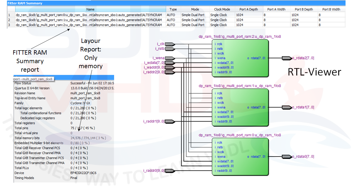
The VHDL code for multi-port RAM instantiates 3 simple dual port RAM.
The dual port RAM are generated using the MegaWizard Plug-Ins in Quartus II software as shown in Figure 3
The dual port ram is generated using different write and read clock. In the VHDL code of multi-port RAM, the write and read clock are connected to the same input clock signal generating a single clock domain. Figure 4 reports the RTL-viewer of Altera Quartus II of the multi-port RAM VHDL implementation.
As clear the dual clock RAM has its read and write clock input connected to the same input clock. In the RTL view is reported the VHDL wrapper of the dual port memory. If you need to use another technology, for instance, Xilinx or ASIC technology, you can use the same VHDL code just simply replacing the dual port memory generated in Altera technology with the new one.
This is a fast and easy way to implement a portable VHDL code even when you should use an internal proprietary macro.
You can use also implement the dual port RAM directly in VHDL.
Here below there is an example of wrapper VHDL code for the dual port memory used in the multi-port memory implementation. The component “alt_dp_ram_1kx8” is the dual port memory generated using the MegaWizard Plug-Ins as in Figure 3
library IEEE;
use IEEE.std_logic_1164.all;
use IEEE.numeric_std.all;

entity dp_ram_1kx8 is
port (
  i_rclk         : in  std_logic;
  i_wclk         : in  std_logic;
  i_rstb         : in  std_logic;
  -- write port
  i_wdata        : in  std_logic_vector( 7 downto 0);
  i_waddr        : in  std_logic_vector( 9 downto 0);
  i_wena         : in  std_logic;
  -- read port
  o_rdata        : out std_logic_vector( 7 downto 0);
  i_raddr        : in  std_logic_vector( 9 downto 0));
end dp_ram_1kx8;

architecture rtl of dp_ram_1kx8 is

component alt_dp_ram_1kx8
PORT
(
  data          : IN STD_LOGIC_VECTOR (7 DOWNTO 0);
  inclock       : IN STD_LOGIC  := '1';
  outclock      : IN STD_LOGIC ;
  rdaddress     : IN STD_LOGIC_VECTOR (9 DOWNTO 0);
  wraddress     : IN STD_LOGIC_VECTOR (9 DOWNTO 0);
  wren          : IN STD_LOGIC  := '0';
  q             : OUT STD_LOGIC_VECTOR (7 DOWNTO 0)
);
end component;

begin

u_alt_dp_ram_1kx8 : alt_dp_ram_1kx8
PORT map
(
  data        =>  i_wdata          ,
  inclock     =>  i_wclk           ,
  outclock    =>  i_rclk           ,
  rdaddress   =>  i_raddr          ,
  wraddress   =>  i_waddr          ,
  wren        =>  i_wena           ,
  q           =>  o_rdata
);
end rtl;
Conclusion
In this post, we got an example of a possible implementation of the VHDL code for multi-port memory.
As clear from the discussion above the strategy is to parallelize the number of RAM block, writing the same data to all dual-port and using different read address to allow multiple different RAM data read at the same time.
The RAM parallelization will, of course, increase the number of RAM block used as in Figure 4.
If we use simple dual port RAM, the number of block RAM overhead is equal to the number of multiple reads we need.
Using true dual port RAM we can optimize the number of RAM used taking advantage of the read port in the write side of the dual-port RAM.
References
[1] https://www.altera.com/content/dam/altera-www/global/en_US/pdfs/literature/ug/ug_ram_rom.pdf
[2] https://www.altera.com/content/dam/altera-www/global/en_US/pdfs/literature/ug/ug_ram.pdf
[3] https://www.xilinx.com/products/design-tools/coregen.html
[4] https://www.altera.com/products/intellectual-property/megawizard.html
If you appreciated this post, please help us to share it with your friend.
[social_sharing style=”style-7″ fb_like_url=”https://surf-vhdl.com/how-to-implement-a-multi-port-memory-on-fpga/” fb_color=”light” fb_lang=”en_US” fb_text=”like” fb_button_text=”Share” tw_lang=”en” tw_url=”https://surf-vhdl.com/how-to-implement-a-multi-port-memory-on-fpga/” tw_button_text=”Share” g_url=”https://surf-vhdl.com/how-to-implement-a-multi-port-memory-on-fpga/” g_lang=”en-GB” g_button_text=”Share” linkedin_url=”https://surf-vhdl.com/how-to-implement-a-multi-port-memory-on-fpga/” linkedin_lang=”en_US” alignment=”center”]
If you need to contact us, please write to: surf.vhdl@gmail.com
We appreciate any of your comment, please post below:
Is it not possible to store this online course so that I can spend more time on this offline . However I appreciate the concept. I do not have the requisite compiler for vhdl and so can not verify the code given above. Thanks for educating me sir. Best regards.
take a look here
https://surf-vhdl.com/how-to-get-free-modelsim-license-and-simulate-your-vhdl-code/